LED (Light-emitting Diode) package unit, package methods thereof, and array area light source

A technology of LED packaging and LED chips, applied in electrical components, circuits, semiconductor devices, etc., can solve the problems of increasing the manufacturing cost of LED light sources to make surface light sources, and achieve the effects of easy implementation, design freedom, and ease of mass production.

Active Publication Date: 2014-04-02
贵州中晟泰科智能技术有限公司
View PDF10 Cites 18 Cited by
  • Summary
  • Abstract
  • Description
  • Claims
  • Application Information

AI Technical Summary

Problems solved by technology

[0004] However, the above-mentioned side-entry light guide module needs to be equipped with light guide plates, diffusion plates, reflectors a

Method used


Image

  • LED (Light-emitting Diode) package unit, package methods thereof, and array area light source
  • LED (Light-emitting Diode) package unit, package methods thereof, and array area light source
  • LED (Light-emitting Diode) package unit, package methods thereof, and array area light source

Examples


Embodiment 1

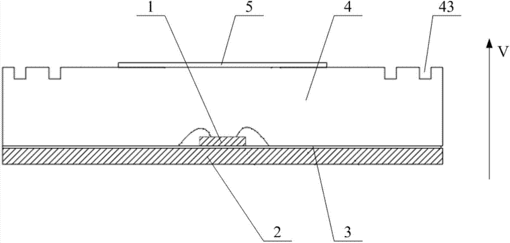
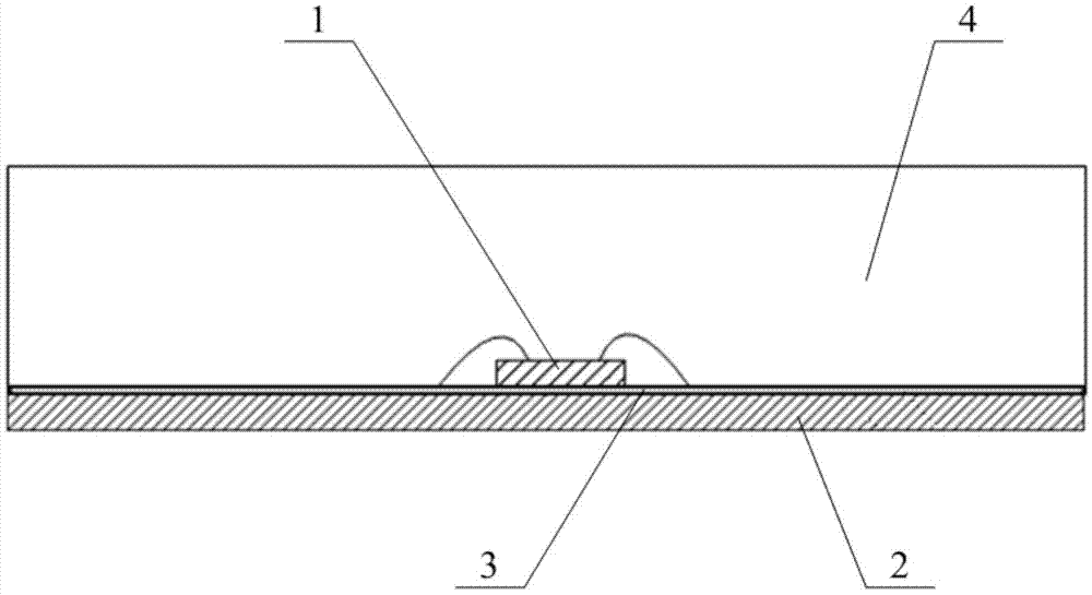
[0082] Such as figure 1 As shown, the LED packaging unit provided in this embodiment includes: an LED chip 1, a substrate 2 for mounting the LED chip 1, the substrate 2 is covered with a light-reflecting layer 3 on the end surface on which the LED chip 1 is mounted, and covers the LED chip 1 And the optical film 4 on the reflective layer 3, the optical film 4 is provided with a reflective sheet 5 corresponding to the LED chip 1 on the vertical upper surface of the optical film 4, and a scattering member for uniformly scattering the light emitted by the LED chip 1 .

[0083] It installs the LED chip 1 on the substrate 2 covered with the reflective layer 3, uses the reflective layer 3 and the reflective sheet 5 to reflect the light emitted by the LED chip 1, and uses the scattering member to refract the light emitted by the LED chip 1 and It is uniform surface scattering, so that the point light source formed by the LED chip 1 is converted into a surface light source; compared w...

Embodiment 2

[0092] The LED packaging method provided in this embodiment includes:

[0093] Step 101, manufacturing the substrate 2;

[0094] Step 102, covering the reflective layer 3 on the end surface of the substrate 2 for mounting the LED chip 1;

[0095] Step 103, mounting the LED chip 1 on the substrate 2;

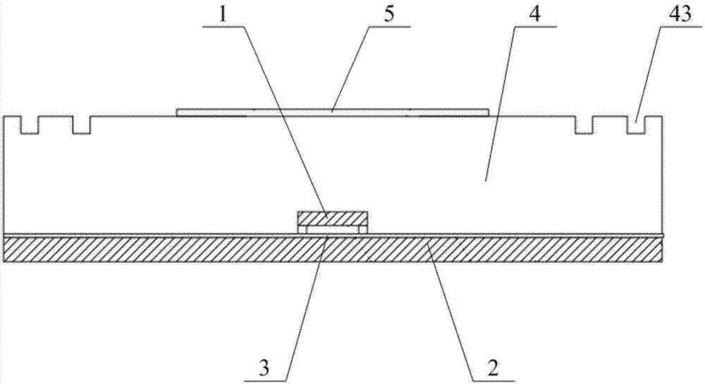
[0096] Step 104, covering the LED chip 1 and the reflective layer 3 with an optical film 4, curing the optical film 4 and forming a blind hole 43 on the vertical upper surface of the optical film 4;

[0097] Step 105 , covering the position of the reflective sheet 5 corresponding to the LED chip 1 on the vertical upper surface of the optical film 4 .

[0098] The LED encapsulation method provided in this embodiment uses the LED encapsulation unit made by this method, by installing the LED chip 1 on the substrate 2 covered with the reflective layer 3, and using the reflective layer 3 and the reflective sheet 5 to emit light from the LED chip 1. The light is reflected, and at th...

Embodiment 3

[0101] The LED packaging method provided in this embodiment includes:

[0102] Step 201, manufacturing the substrate 2;

[0103] Step 202, covering the reflective layer 3 on the end surface of the substrate 2 for mounting the LED chip 1;

[0104] Step 203, mounting the LED chip 1 on the substrate 2;

[0105] Step 204, covering the optical film 4 on the LED chip 1 and the reflective layer 3;

[0106] Step 205, before the optical film 4 is cured, form a blind hole 43 on the vertical upper surface of the optical film 4 through the mold 6;

[0107] Step 206 , covering the position of the reflective sheet 5 corresponding to the LED chip 1 on the vertical upper surface of the optical film 4 .

[0108] Wherein, step 204 and step 205 can also be replaced by:

[0109] Step 304, covering the optical film 4 on the LED chip 1 and the reflective layer 3;

[0110] Step 305 , after the optical film 4 is cured, a blind hole 43 is formed on the vertical upper surface of the optical film 4...


PUM


Abstract

The invention relates to an LED (Light-emitting Diode) package unit, package methods thereof, and an array area light source. The LED package unit comprises an LED chip, a base plate for installing the LED chip, an optical thin film covering on the LED chip and a reflective layer, and a scattering component for uniformly scattering light emitted by the LED chip, wherein the base plate is covered with the reflective layer on an end face for installing the LED chip; a reflective piece is arranged at a position of the optical thin film along a vertical upper surface, corresponding to the LED chip; compared with an edge LED light guiding module, components such as a light guiding plate and a diffusion plate are omitted, so that the cost for manufacturing an area light source by utilizing the LED chip is effectively reduced. The invention also provides the array area light source, batch production is convenient, and the cost is reduced. The invention also provides two LED package methods, and through utilization of the LED package unit manufactured by the two methods, the cost for manufacturing the area light source by utilizing the LED light source can be effectively reduced.

Description

technical field [0001] The invention relates to the technical field of semiconductor lighting, in particular to an LED packaging unit, a packaging method thereof, and an array surface light source. Background technique [0002] LED light sources have the advantages of long life and power saving, so they are increasingly used in the field of lighting. [0003] As we all know, LED light sources are usually point light sources. At present, the main way to convert the LED light source from a point light source to a surface light source is to use the light guide plate scattering principle to make the LED light source into a surface light source. Its specific structure includes: the frame is made of metal material, and LED light bars as incident light sources are arranged along the inner side of the frame side walls (wherein LED light bars can be set on the inner sides of the four side walls of the frame, or can be arranged on the frame opposite to each other) The inner sides of...

Claims


Application Information

Patent Timeline
IPC IPC(8): H01L33/62H01L33/60
CPCH01L33/58H01L33/60H01L2933/0058H01L2933/0091
Inventor 韦嘉梁润园黄超袁长安张国旗
Owner 贵州中晟泰科智能技术有限公司
Why Eureka
Try Eureka