

Touch display panel and manufacturing method thereof
A technology of touch display panel and touch control, which is applied in the direction of exposure device, optics, instrument, etc. of photographic plate making process, which can solve the problems of unfavorable process simplification, influence of touch screen display effect, display effect influence, etc., and achieve favorable Light and thin, good display effect, effect of reducing thickness
- Summary
- Abstract
- Description
- Claims
- Application Information
AI Technical Summary
Problems solved by technology
Method used
Image

Examples
Embodiment Construction
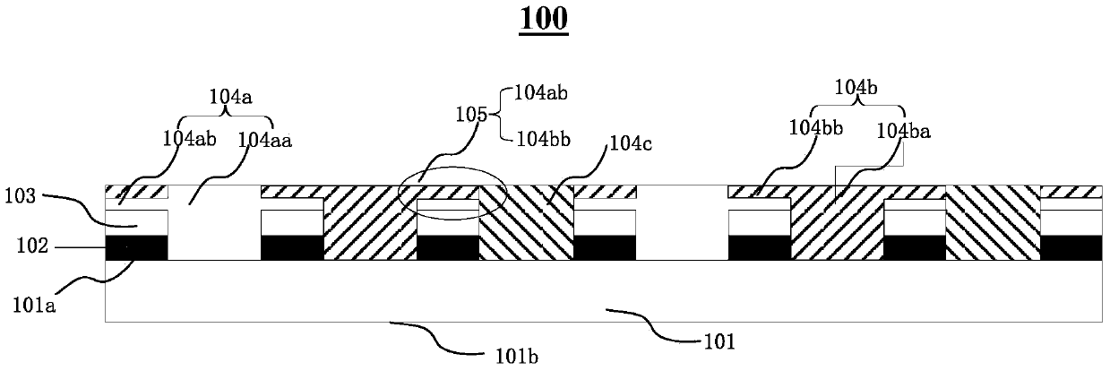
[0024] In order to illustrate the touch display panel provided by the present invention and the manufacturing method thereof, a detailed description will be given below in conjunction with the accompanying drawings and text descriptions of the specification.
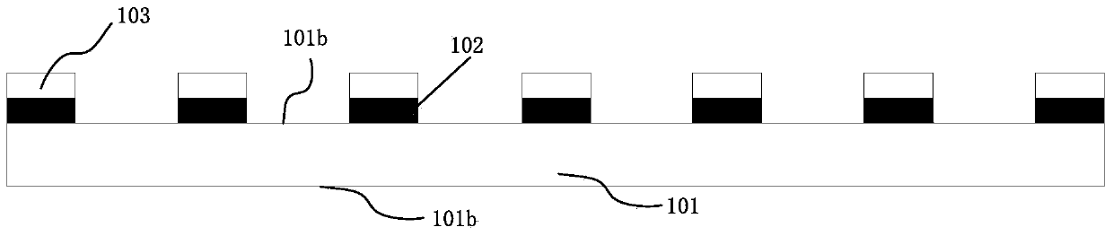
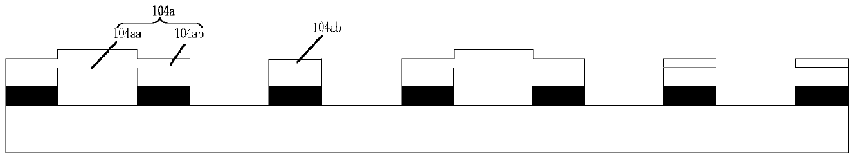
[0025] Please refer tofigure 1 , which is a schematic cross-sectional view of the touch substrate 100 of the touch display panel according to a preferred embodiment of the present invention. The touch display screen includes a touch substrate 100, a driving substrate (not shown in the figure) and a functional display layer (not shown in the figure), the touch substrate 100 and the driving substrate are relatively spaced apart, and the functional display layer The layer is disposed between the touch substrate 100 and the driving substrate. In this embodiment, the touch display is a touch liquid crystal display, the driving substrate is a TFT array substrate, and the functional display layer is a liquid crystal layer. In ...
PUM
 Abstract
Description
Claims
Application Information