Isolation structure of high-voltage driving circuit

A high-voltage drive circuit and isolation structure technology, applied in circuits, electrical components, semiconductor devices, etc., can solve the problem of high electric field peak value and achieve the effect of improving reliability

Active Publication Date: 2014-04-23
WUXI CHIPOWN MICROELECTRONICS
View PDF3 Cites 11 Cited by
  • Summary
  • Abstract
  • Description
  • Claims
  • Application Information

AI Technical Summary

Problems solved by technology

[0004] The purpose of the present invention is to provide an isolation structure used in a high-voltage drive circuit, which solves the problem that the electric field peak value of the RESURF LDMOS lateral PN junction surface is too high, and improves the reliability of the isolation structure

Method used


Image

  • Isolation structure of high-voltage driving circuit
  • Isolation structure of high-voltage driving circuit
  • Isolation structure of high-voltage driving circuit

Examples


Embodiment Construction

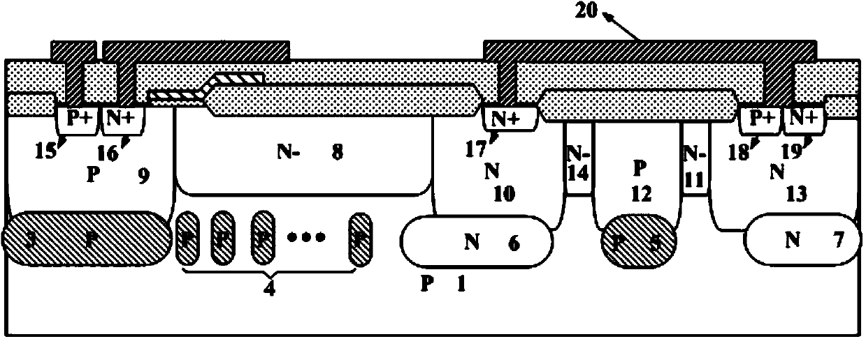
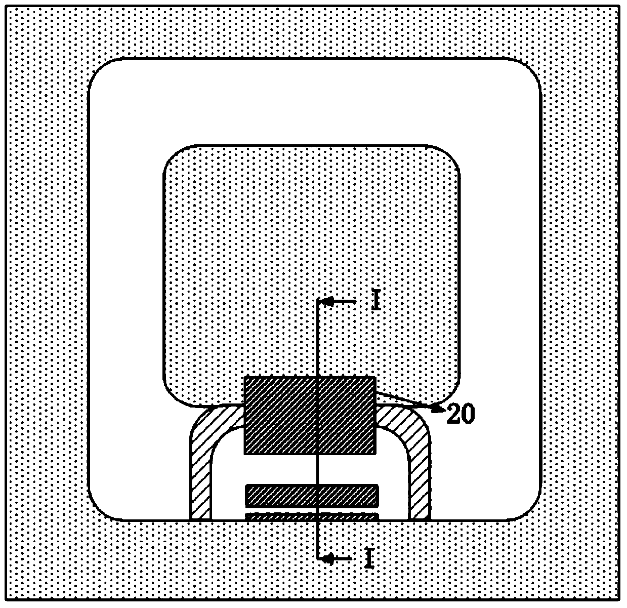
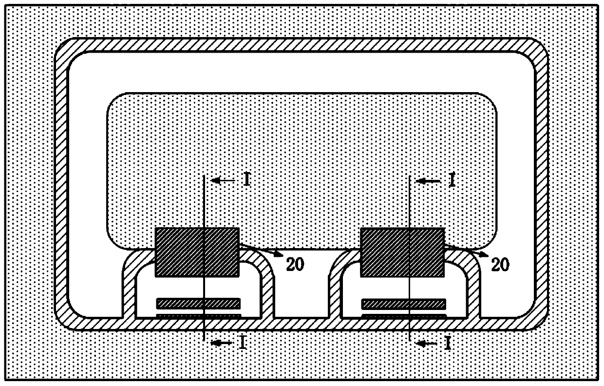
[0024] Such as figure 1 The isolation structure of a high-voltage driving circuit shown includes a P-type substrate 1, and a first P-type buried layer 3, a second P-type interrupted island-shaped buried layer region 4, and a third P-type buried layer are arranged in the P-type substrate 1. type buried layer 5, the first N-type buried layer 6, the second N-type buried layer 7, and the second P-type interrupted island-shaped buried layer region 4 is located between the first P-type buried layer and the first N-type buried layer 6 , the third P-type buried layer 5 is located between the first N-type buried layer 6 and the second N-type buried layer 7 . A first P-type well region 9 is provided on the surface of the P-type substrate 1 , and the lower part of the first P-type well region 9 is connected to the first P-type buried layer 3 . A first N-type well region 8 is provided on the surface of the P-type substrate 1, the first N-type well region 8 is connected to the first P-ty...


PUM


Abstract

The invention discloses an isolation structure of a high-voltage driving circuit. The isolation structure comprises a P type substrate, wherein a first P type buried layer, a second P type intermittent island buried layer area, a third P type buried layer, a first N type buried layer and a second N type buried layer; the second P type intermittent island buried layer area is located between the first P type buried layer and the first N type buried layer; the third P type buried layer is located between the first N type buried layer and the second N type buried layer. According to the isolation structure, the problem that the peak value of the surface electric field of the transverse PN junction of RESURFLDMOS is overhigh is solved, and the reliability of the isolation structure is improved.

Description

technical field [0001] The invention relates to the field of power semiconductor integrated circuits, and more precisely, relates to an isolation structure of a high-voltage driving circuit. Background technique [0002] High-voltage drive circuits are used in various fields such as motor drives, electronic rectifiers in fluorescent lamps, and power management. The level shift circuit in the high-voltage drive circuit is a key part of the entire circuit. The electrical performance of the high-voltage insulated gate field effect transistor LDMOS and the electrical coupling between the high-voltage LDMOS that make up the level shift circuit will affect the performance of the shift circuit. The source of the high-voltage LDMOS The large current and high voltage at the drain terminal will also cause parasitic effects in other areas of the entire integrated circuit and affect the electrical performance of the entire drive circuit. Therefore, the electrical performance of the high...

Claims


Application Information

Patent Timeline
Patent Type & Authority Applications(China)
IPC IPC(8): H01L29/06H01L29/78
CPCH01L29/7835H01L29/1083H01L29/42368H01L29/0634H01L29/7816
Inventor 易扬波李海松陶平陈健张立新吴虹王钦
Owner WUXI CHIPOWN MICROELECTRONICS
Why Eureka
Try Eureka