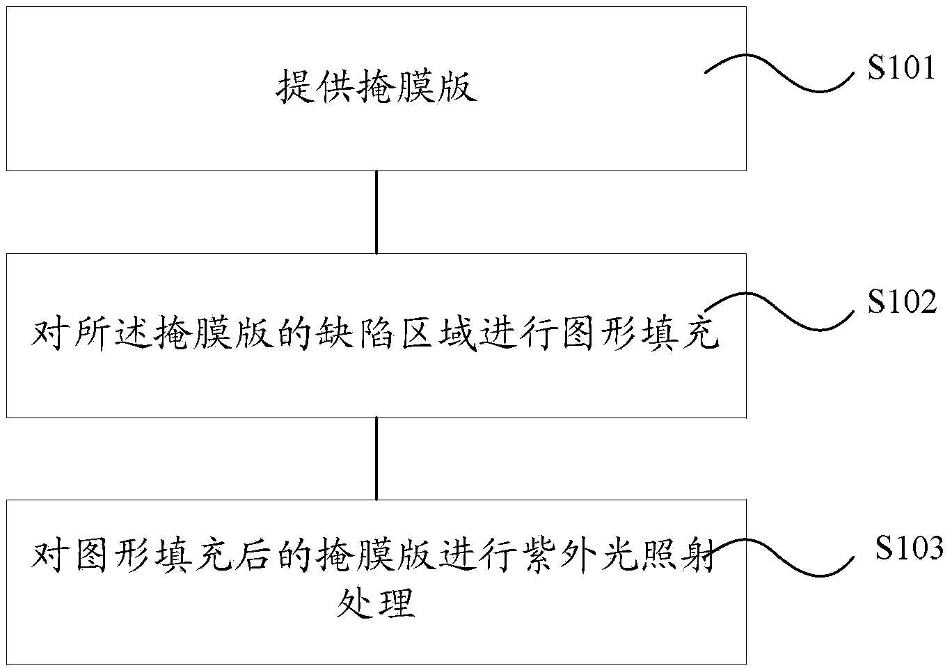
Mask repair method

A repairing method and a technology of a mask plate, which are applied in the direction of photolithography, optics, instruments, etc. on the pattern surface, can solve the problems of low efficiency and poor effect of the repairing method, so as to prevent the defects from becoming serious, save production costs, reduce The effect of dealing with risk

Inactive Publication Date: 2014-05-07
SEMICON MFG INT (SHANGHAI) CORP
View PDF8 Cites 7 Cited by
  • Summary
  • Abstract
  • Description
  • Claims
  • Application Information

AI Technical Summary

Problems solved by technology

[0005] The purpose of the present invention is to provide a mask repair method to solve the problem of low efficiency and poor effect of the repair method in the prior art

Method used


Image

  • Mask repair method
  • Mask repair method
  • Mask repair method

Examples


Embodiment 1

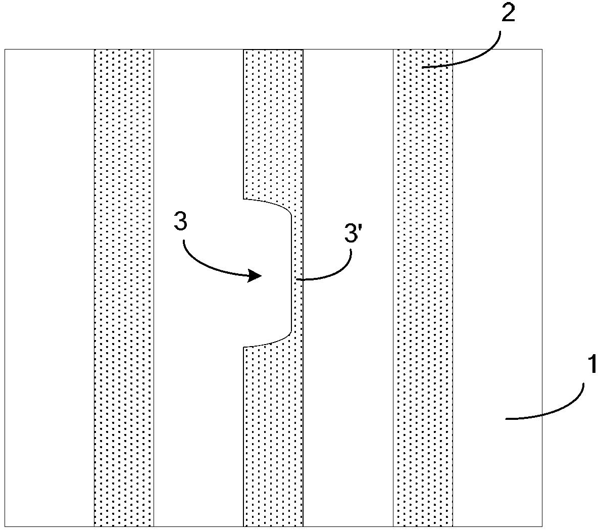
[0035] Please refer to figure 2 , the defective mask includes a substrate 1 and a patterned light-shielding layer 2, as shown in the figure, this mask is a line (Line) mask, which is used in the semiconductor manufacturing process metal layer. E.g figure 2 The line in the middle has a pattern missing 3. In this case, it must be repaired, otherwise after the photolithography process, figure 2 The narrow line part 3' corresponding to the lack of 3 in the figure shown in the figure cannot be formed on the silicon wafer, and then there is a fracture phenomenon, forming a dead unit (dead die).

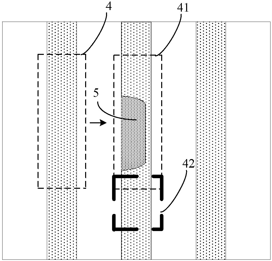
[0036] Please refer to image 3 , copy a normal region 4 from a nearby pattern with the same structure to the missing part of the defect region to obtain the region 5 to be filled, the effective size of the normal region 4 should be greater than the area of ​​the missing pattern, so that the area to be filled can be accurately obtained area 5. During copying, the copied normal area ...

Embodiment 2

[0042] The difference between this embodiment and Embodiment 1 is that the masks processed are different, please refer to Figure 7 , the defective mask is a square mask, which is used to form a through hole (contact) on a silicon wafer. As shown in the figure, the normal area is a pattern 8, and in this embodiment, the middle defective area has a pattern 8'.

[0043] Please refer to Figure 8 , using the same method as in Embodiment 1, copying the normal area (the pattern 81 is selected here) to the defect area to obtain the area 9 to be filled. Likewise, the replicated normal area 81' should match the surrounding normal area. For example, the position of the copied normal region 81 ′ can be positioned based on the straight lines x and y formed by the graphic edges of the surrounding normal regions.

[0044] Please refer to Figure 9 , using FIB to deposit naphthalene into the area to be filled to form the repaired area 10 . For the same reason, residual defects 11 are f...


PUM

PropertyMeasurementUnit
wavelengthaaaaaaaaaa
poweraaaaaaaaaa

Abstract

The invention discloses a mask repair method. According to the mask repair method, a halo residual defect generated after pattern deletion of a mask is treated with ultraviolet light for repairing; as the ultraviolet light is short in wave length and high in energy, the halo residual defect is stimulated to decompose in a short time, and then disappears. Moreover, as the phase position layer of the mask cannot be damaged by ultraviolet light, the treating risk is reduced, the residual defect is prevented from getting worse due to large quantity of cargo passing use in the practical production, the service life is greatly prolonged, and the production cost is reduced.

Description

technical field [0001] The invention relates to the field of integrated circuit manufacturing, in particular to a method for repairing a mask plate. Background technique [0002] In the semiconductor manufacturing process, the lithography process has always been a very important link, and the mask plate occupies a pivotal position in the lithography. A common mask includes a transparent substrate, such as a quartz substrate, and a light-shielding layer on the substrate. Usually, the light-shielding layer needs to contain metal. The mask is to make the patterns required in the semiconductor manufacturing process on the light-shielding layer , so that the pattern is formed on the silicon wafer through a series of processes. [0003] In the process of making the mask, usually due to various unmeasurable factors, such as a series of problems such as the environment, the texture of the quartz substrate, and photoresist, the manufactured mask will have defects, and usually the ma...

Claims


Application Information

Patent Timeline
Patent Type & Authority Applications(China)
IPC IPC(8): G03F1/72G03F1/74
Inventor 吴苇
Owner SEMICON MFG INT (SHANGHAI) CORP
Why Eureka
Try Eureka