Array substrate, manufacturing method thereof and display device

A technology of array substrates and substrates, which is used in semiconductor/solid-state device manufacturing, instruments, semiconductor devices, etc., and can solve problems such as affecting display effects, image differences, and different transmittances.

Active Publication Date: 2014-05-14
BOE TECH GRP CO LTD
View PDF5 Cites 13 Cited by
  • Summary
  • Abstract
  • Description
  • Claims
  • Application Information

AI Technical Summary

Problems solved by technology

The backlight source of TFT-LCD is white light, which is usually composed of three primary colors of red, green and blue. The white light becomes linearly polarized white light after passing through the polarizer on the array substrate side, and the linearly polarized light is polarized after passing through the liquid crystal layer. The direction is affected by the thickness of the liquid crystal layer and the deflection angle of the liquid crystal. Generally, the pixel electrodes or common electrodes corresponding to the red, green, and blue sub-pixel units in the LCD have the same structure and the same voltage, so that the red, green, and blue sub-pixel units The deflection angle of the liquid crystal is the same, so when the white light passes through the liquid crystal lay

Method used


Image

  • Array substrate, manufacturing method thereof and display device
  • Array substrate, manufacturing method thereof and display device
  • Array substrate, manufacturing method thereof and display device

Examples


Embodiment Construction

[0042]The following will clearly and completely describe the technical solutions in the embodiments of the present invention with reference to the accompanying drawings in the embodiments of the present invention. Obviously, the described embodiments are only some, not all, embodiments of the present invention. Based on the embodiments of the present invention, all other embodiments obtained by persons of ordinary skill in the art without making creative efforts belong to the protection scope of the present invention.

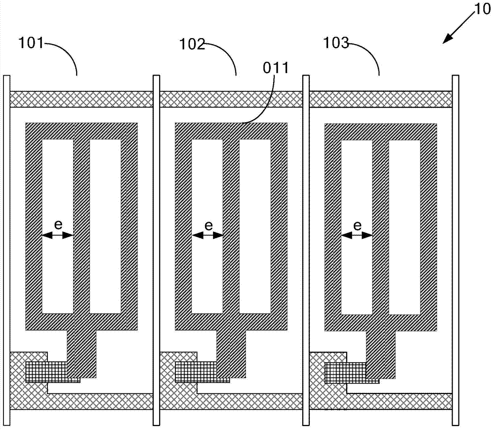
[0043] In the prior art, the array substrate includes a plurality of pixel units arranged in an array, and the structure of the pixel units is as follows: figure 1 as shown, figure 1 The illustrated pixel unit 10 includes three sub-pixel units, respectively a red sub-pixel unit 101, a green sub-pixel unit 102, and a blue sub-pixel unit 103, wherein each sub-pixel unit corresponds to a first electrode 011, and the first electrode 011 includes three strip struct...


PUM


Abstract

The embodiment of the invention provides an array substrate, a manufacturing method thereof and a display device, and relates to the technical field of display. The color cast phenomenon of the display device can be reduced, and the display effect can be improved. The array substrate comprises a plurality of pixel units which are arranged in an array mode, each pixel unit comprises a plurality of sub-pixel units, the widths of the sub-pixel units are equal, each sub-pixel unit corresponds to one first electrode, each first electrode comprises a plurality of strip-shaped structures which are arranged at an equal interval, and intervals of the strip-shaped structures of the first electrodes corresponding to different sub-pixel units in each pixel unit are not completely equal; any sub-pixel unit meets the inequation of Q*W+ (Q-1)*D<A, wherein A is the width of the sub-pixel units, Q is the number of the strip-shaped structures of the first electrodes corresponding to the sub-pixel units, D is the interval of the strip-shaped structures of the first electrodes corresponding to the sub-pixel units, and W is the with of the strip-shaped structures of the first electrodes corresponding to the sub-pixel units. The array substrate, the manufacturing method of the array substrate and the display device are applied to the technical field of display.

Description

technical field [0001] The present invention relates to the field of display technology, in particular to an array substrate, a preparation method thereof, and a display device. Background technique [0002] The liquid crystal panel in TFT-LCD (Thin Film Transistor-Liquid Crystal Display, thin film transistor liquid crystal display device) is mainly composed of an array substrate, a color filter substrate and a liquid crystal layer between the array substrate and the color filter substrate. Two polarizers whose polarization directions are completely perpendicular are respectively arranged on the substrate. When the TFT-LCD is working, the light emitted by the backlight illuminates the array substrate, and the transmittance of the light through the liquid crystal layer and the color substrate is determined according to the image data input to the TFT-LCD. The display panel can display different colors according to different transmittances. Color grayscale, and display the im...

Claims


Application Information

Patent Timeline
IPC IPC(8): G02F1/1343G02F1/1362G02F1/1368H01L27/12H01L21/77
CPCG02F1/133707G02F1/134363G02F1/134372H01L27/12G02F1/1368H01L27/124H01L27/1259
Inventor 徐智强金熙哲徐超
Owner BOE TECH GRP CO LTD
Why Eureka
Try Eureka