Multilayer wiring substrate
A multi-layer wiring substrate and insulating layer technology, applied in the direction of multi-layer circuit manufacturing, electrical components, printed circuit components, etc., can solve the problem of inability to obtain adhesion, and achieve the effect of preventing peeling
- Summary
- Abstract
- Description
- Claims
- Application Information
AI Technical Summary
Problems solved by technology
Method used
Image

Examples
Embodiment Construction
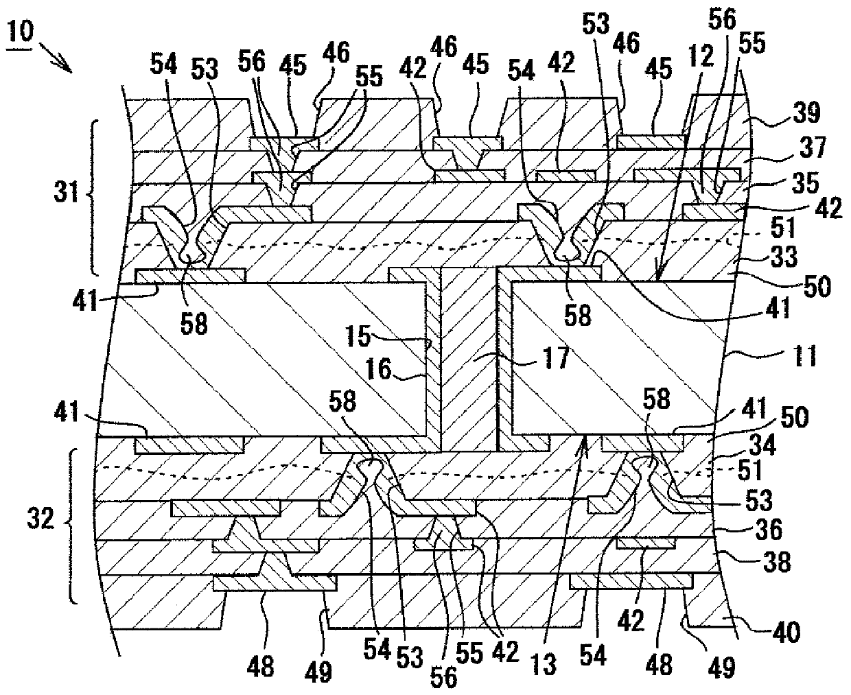
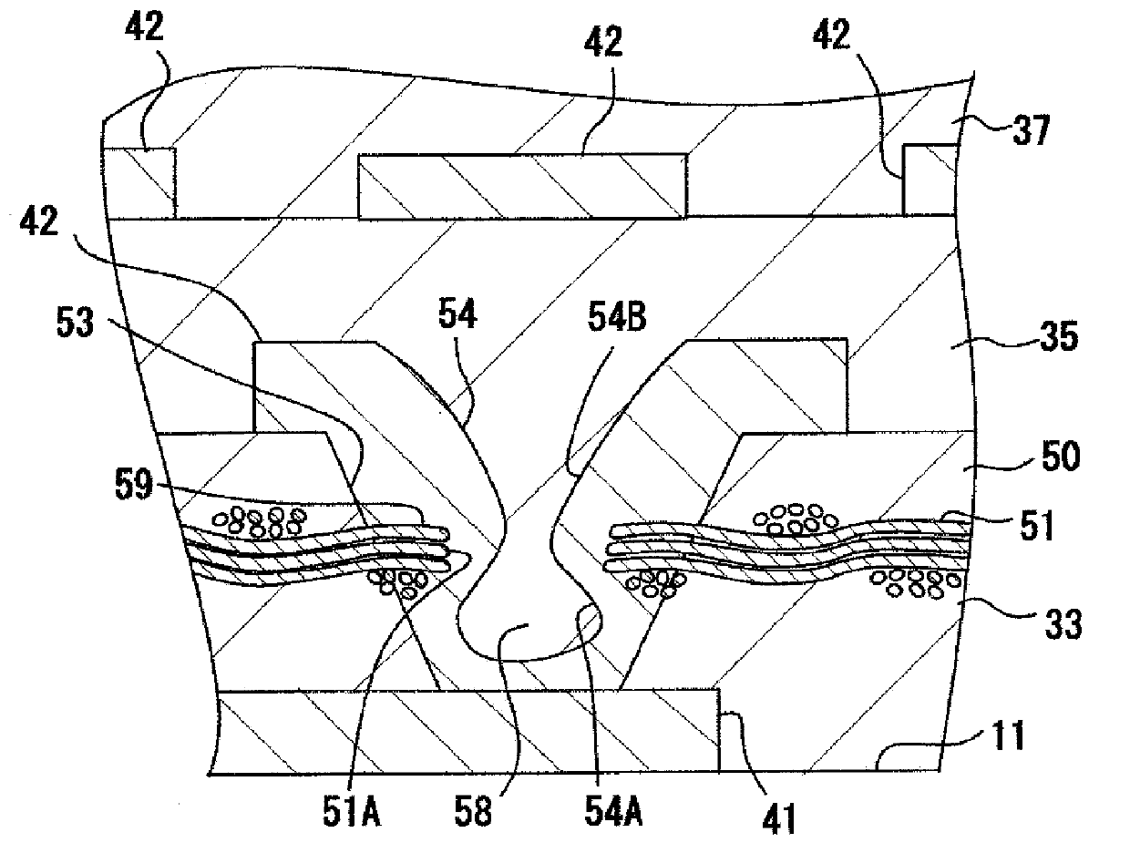
[0031] Hereinafter, an embodiment in which the present invention is embodied in a multilayer wiring board will be described in detail with reference to the drawings.
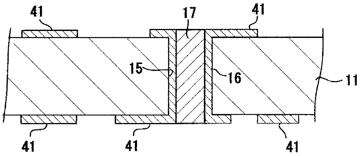
[0032] Such as figure 1 As shown, the multilayer wiring substrate 10 of the present embodiment includes a core substrate 11, a core main surface 12 formed on the core substrate 11 ( figure 1 The first buildup layer 31 on the upper surface) and the core back surface 13 formed on the core substrate 11 ( figure 1 The middle is the second build-up layer 32 on the lower surface).
[0033] The core substrate 11 is constituted by, for example, a resin insulating material (glass epoxy resin material) obtained by impregnating glass fiber cloth as a reinforcing material with epoxy resin. Conduction holes 15 (through holes) penetrating through the core substrate 11 in the thickness direction are formed at a plurality of locations on the core substrate 11 , and via conductors 16 are formed in the conduction holes 15 . ...
PUM
 Abstract
Description
Claims
Application Information
 - R&D
- Intellectual Property
- Life Sciences
- Materials
- Tech Scout
- Unparalleled Data Quality
- Higher Quality Content
- 60% Fewer Hallucinations
Browse by: Latest US Patents, China's latest patents, Technical Efficacy Thesaurus, Application Domain, Technology Topic, Popular Technical Reports.
© 2025 PatSnap. All rights reserved.Legal|Privacy policy|Modern Slavery Act Transparency Statement|Sitemap|About US| Contact US: help@patsnap.com