Fin type field effect transistor forming method

A fin field effect transistor and fin technology, applied in the direction of electrical components, semiconductor/solid-state device manufacturing, semiconductor devices, etc., can solve the problems of fin field effect transistor threshold voltage offset, fin 11 damage, error, etc., Achieve the effect of avoiding threshold voltage shift, improving stability and good uniformity

Active Publication Date: 2014-05-21
SEMICON MFG INT (SHANGHAI) CORP
View PDF4 Cites 3 Cited by
  • Summary
  • Abstract
  • Description
  • Claims
  • Application Information

AI Technical Summary

Problems solved by technology

[0006] In the prior art, the fin 11 in the fin field effect transistor is mainly formed by dry etching the semiconductor substrate 10. However, due to certain errors in the etching process, it is difficult to precisely control the thickness of the formed fin 11. The electrical properties of each fin field effect transistor formed are too di...

Method used


Image

  • Fin type field effect transistor forming method
  • Fin type field effect transistor forming method
  • Fin type field effect transistor forming method

Examples


Embodiment Construction

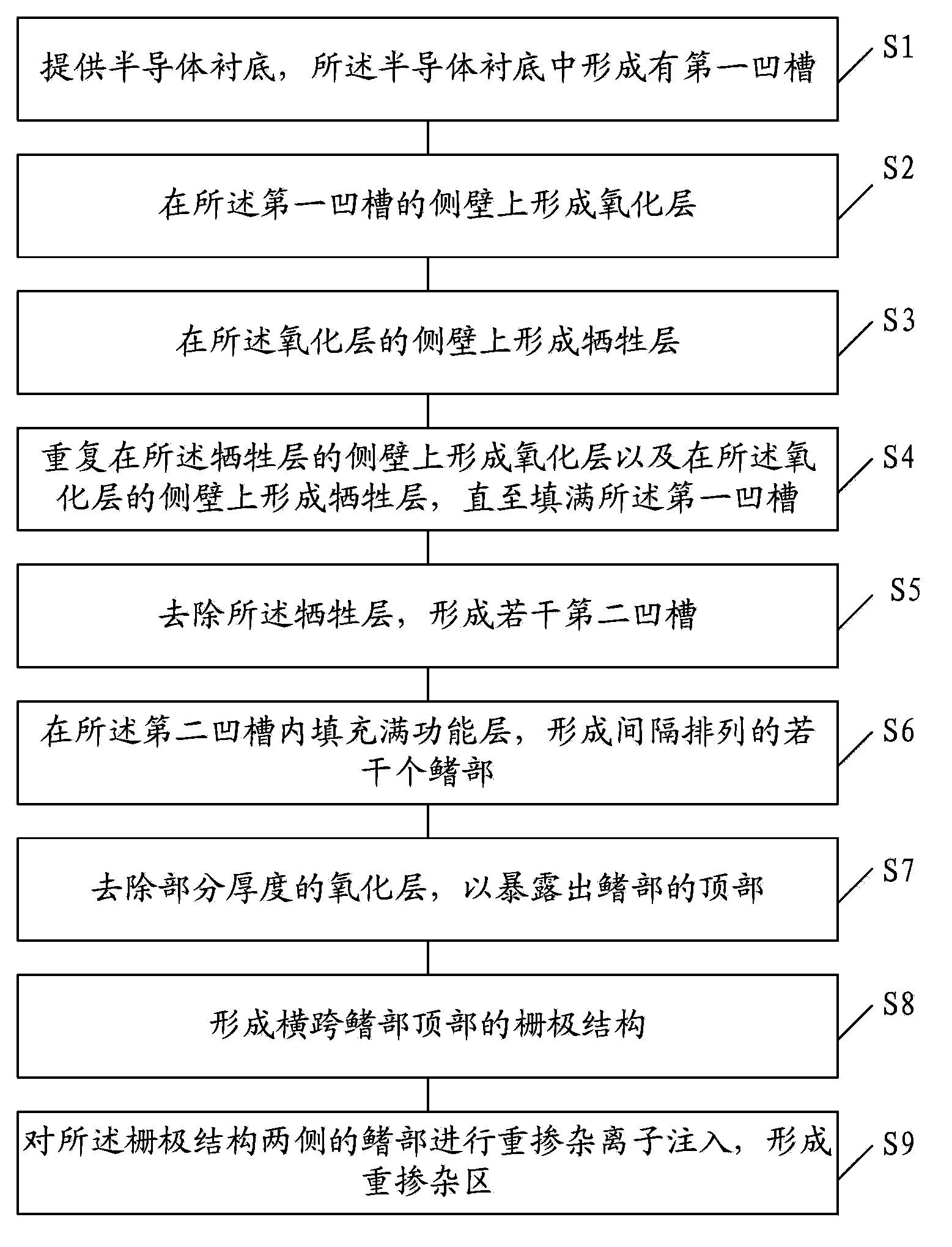
[0019] In order to make the above objects, features and advantages of the present invention more comprehensible, specific implementations of the present invention will be described in detail below in conjunction with the accompanying drawings.

[0020] In the following description, many specific details are set forth in order to fully understand the present invention, but the present invention can also be implemented in other ways than those described here, so the present invention is not limited by the specific embodiments disclosed below.

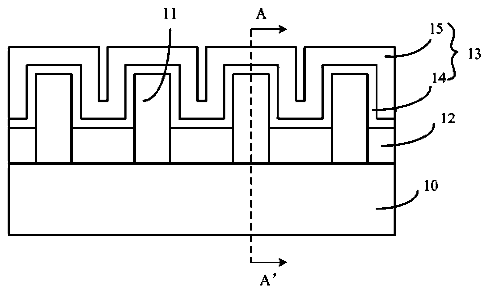
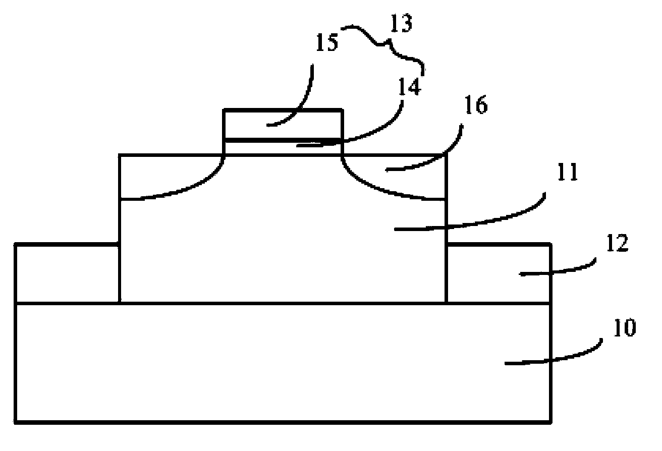
[0021] As mentioned in the background technology section, in the prior art, when the fins of the fin field effect transistors are formed by dry etching the semiconductor substrate, the thickness of the formed fins cannot be precisely controlled, and the formed fin field effect transistors are The difference in electrical performance due to different channel widths; moreover, the dry etching process will cause damage to the surface of the f...


PUM

PropertyMeasurementUnit
Thicknessaaaaaaaaaa
Heightaaaaaaaaaa

Abstract

A fin type field effect transistor forming method comprises providing a semiconductor substrate with a first groove formed inside; sequentially forming into a plurality of oxidation layers and a plurality of sacrificial layers in an interval mode inside the first groove from the lateral wall of the first groove to the center until the first groove is filled; removing the sacrificial layers which are arranged between the oxidation layers to form into a plurality of second grooves; enabling the second groove to be filled with functional layers to form into a plurality of fin portions which are arranged in an interval mode. The fin type field effect transistor forming method can accurately control the fin portion thickness of the fin type field effect transistor, improve the fin portion surface uniformity and accordingly improve the stability of the formed fin type field effect transistor.

Description

technical field [0001] The invention relates to the technical field of semiconductor manufacturing, in particular to a method for forming a fin field effect transistor. Background technique [0002] With the rapid development of semiconductor manufacturing technology, semiconductor devices are developing towards higher element density and higher integration. As the most basic semiconductor device, transistors are currently being widely used. With the increase of component density and integration of semiconductor devices, the gate size of transistors is getting shorter and shorter. The shortening of gate size of transistors will lead to short The channeling effect, which in turn generates leakage current, ultimately affects the electrical performance of semiconductor devices. [0003] In order to overcome the short channel effect of the transistor and suppress the leakage current, the prior art proposes a Fin Field Effect Transistor (Fin FET), please refer to figure 1 and ...

Claims


Application Information

Patent Timeline
IPC IPC(8): H01L21/28H01L21/336
CPCH01L29/66795H01L29/785H01L29/7851
Inventor 禹国宾
Owner SEMICON MFG INT (SHANGHAI) CORP
Why Eureka
Try Eureka