Method For Fabricating Semiconductor Package

A semiconductor and packaging technology, applied in the field of semiconductor packaging manufacturing methods, can solve the problems of semiconductor chip offset, manufacturing cost cannot be reduced, redistribution circuit layer offset chip electrical connection, etc., to improve product yield. Effect

Inactive Publication Date: 2014-05-21
SILICONWARE PRECISION IND CO LTD
View PDF7 Cites 4 Cited by
  • Summary
  • Abstract
  • Description
  • Claims
  • Application Information

AI Technical Summary

Problems solved by technology

[0009] However, when the semiconductor chip is pasted on the heat release tape in the aforementioned existing semiconductor package manufacturing method, it is easy to cause the semiconductor chip to shift due to the thermal expansion coefficient of the heat release tape and the impact of the mold flow during molding. The problem is that when the redistribution layer is produced later, due to the offset of the chip, part of the redistribution layer is not electrically connected to the chip due to the offset, which leads to poor reliability of the product. Therefore, the use of this heat release tape will also leading to the inability to reduce the manufacturing cost

Method used


Image

  • Method For Fabricating Semiconductor Package
  • Method For Fabricating Semiconductor Package
  • Method For Fabricating Semiconductor Package

Examples


no. 1 example

[0053] The following will match Figure 2A to Figure 2H A schematic cross-sectional view of the first embodiment of the manufacturing method of the semiconductor package of the present invention is described in detail.

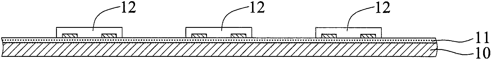
[0054] Such as Figure 2A As shown, a carrier plate 20 is provided, and a release layer 21 is formed on the carrier plate 20, and the material of the carrier plate 20 is glass, and the material of the release layer 21 is amorphous silicon (Amorphous Silicon), Parylene or amorphous phase-silicon dioxide (α-SiO 2 ), the release layer 21 can be formed by chemical vapor deposition (Chemical Vapor Deposition, CVD).

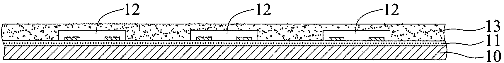
[0055] Such as Figure 2B As shown, a metal layer 22 is formed on the release layer 21, and is formed by, for example, plasma-assisted chemical vapor deposition (Plasma Enhance Chemical Vapor Deposition, PECVD), chemical vapor deposition (Chemical Vapor Deposition, CVD), physical vapor deposition (Physical The metal layer 22 is formed by Vapor Depo...

no. 2 example

[0064] see image 3 , which is a schematic cross-sectional view of the second embodiment of the manufacturing method of the semiconductor package of the present invention.

[0065] This embodiment is substantially the same as the previous embodiment, the main difference is that this embodiment does not use the metal layer 22, but the adhesive layer 23' used is distributed with a plurality of metal particles, and the metal particles are used to block the The light a passes through the adhesive layer 23 ′, and other steps in this embodiment are similar to those in the previous embodiment, so details are not repeated here.

no. 3 example

[0067] see Figure 4 , which is a schematic cross-sectional view of the third embodiment of the manufacturing method of the semiconductor package of the present invention.

[0068] This embodiment is substantially the same as the second embodiment, and the main difference is that the metal particles 30 of this embodiment are composed of silicon oxide spheres 30a and a metal coating layer 30b formed on the surface of the silicon oxide spheres 30a. The metal particles 30 can block the light a from passing through the adhesive layer 23 ′, and other steps of this embodiment are similar to those of the second embodiment, so details are not repeated here.


PUM


Abstract

A method for fabricating a semiconductor package is disclosed, which includes the steps of: providing a carrier having a release layer and an adhesive layer sequentially formed thereon; disposing a plurality of semiconductor chips on the adhesive layer; forming an encapsulant on the adhesive layer for encapsulating the semiconductor chips; disposing a substrate on the encapsulant; exposing the release layer to light through the carrier so as to remove the release layer and the carrier; and then removing the adhesive layer, thereby effectively preventing the semiconductor chips from being exposed to light so as to avoid any photo damage to the semiconductor chips.

Description

technical field [0001] The present invention relates to a method for manufacturing a semiconductor package, in particular to a method for manufacturing a semiconductor package that prevents light from damaging semiconductor chips. Background technique [0002] Nowadays, with the advancement of science and technology, manufacturers of electronic products have developed semiconductor packages with various embodiments. At present, the size of semiconductor chips tends to be miniaturized. Therefore, it is necessary to continuously improve and overcome the process technology of semiconductor packages. , in order to cooperate with miniaturized semiconductor chips, and conform to the trend of modern technology products to be thin, light and small. [0003] see Figure 1A to Figure 1E , which is a schematic cross-sectional view of a manufacturing method of a semiconductor package in the prior US Patent No. 7202107. [0004] Such as Figure 1A As shown, a carrier board 10 is provid...

Claims


Application Information

Patent Timeline
Patent Type & Authority Applications(China)
IPC IPC(8): H01L21/56
CPCH01L21/568H01L21/6835H01L2221/68381H01L21/561H01L23/3121H01L24/96H01L2924/12042H01L2924/00
Inventor 纪杰元黄荣邦陈彦亨许习彰张江城邱世冠
Owner SILICONWARE PRECISION IND CO LTD
Why Eureka
Try Eureka