Light emitting device and related projection system thereof

A light-emitting device and excitation light technology, which is applied to lighting devices, projection devices, lighting device components, etc., can solve the problem of large loss of laser light

Active Publication Date: 2014-06-04
APPOTRONICS CORP LTD
View PDF8 Cites 22 Cited by
  • Summary
  • Abstract
  • Description
  • Claims
  • Application Information

AI Technical Summary

Problems solved by technology

However, the angle range in which the collecting lens can collect light beams is generally 65 degrees to 75 degrees. In this way, t

Method used


Image

  • Light emitting device and related projection system thereof
  • Light emitting device and related projection system thereof
  • Light emitting device and related projection system thereof

Examples


Embodiment 1

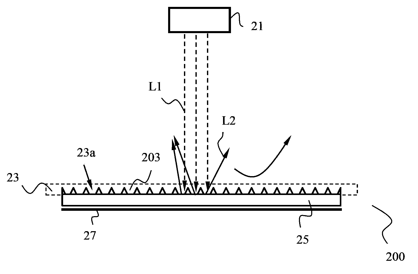
[0024] see Figure 2A , Figure 2B and Figure 2C , Figure 2A is a schematic structural view of an embodiment of the light-emitting device of the present invention, Figure 2B yes Figure 2A The schematic diagram of the local light path structure in the light-emitting device shown, Figure 2C yes Figure 2A Top view of the microstructure layer in the light-emitting device shown. . The light emitting device 200 includes an excitation light source 21 and a wavelength conversion device 22 , wherein the wavelength conversion device 22 includes a microstructure layer 23 , a wavelength conversion layer 25 and a reflective layer 27 .

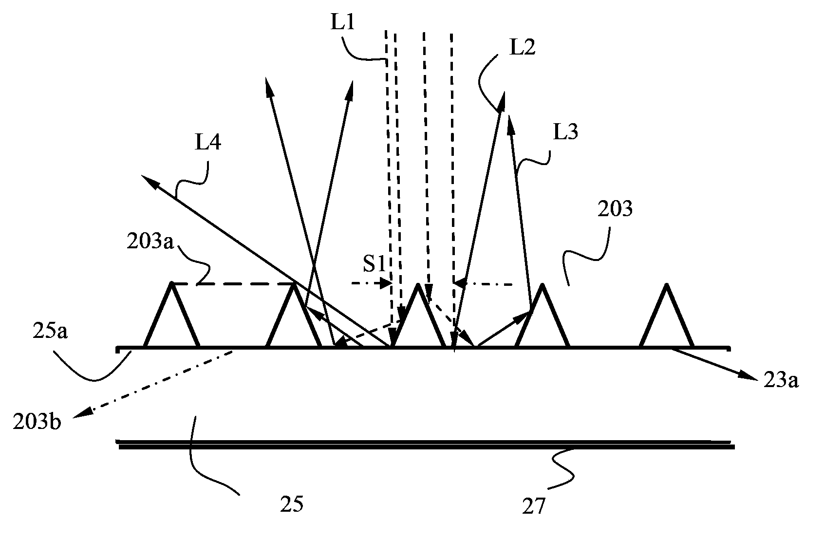
[0025] The microstructure layer 23 includes a microstructure array 23a. Each microstructure 203 in the microstructure array 23a is in the shape of a through hole, and the area of ​​the upper opening 203a of each microstructure 203 is larger than the area of ​​the lower opening 203b, wherein the upper opening 203a of each microstructure is loca...

Embodiment 2

[0045] see Figure 3A and Figure 3B , Figure 3A is a schematic structural view of an embodiment of the light-emitting device of the present invention, Figure 3B yes Figure 3A Top view of the wavelength conversion device in the light emitting device shown. The light emitting device 300 includes an excitation light source 31 and a wavelength conversion device 32 , wherein the wavelength conversion device 32 includes a microstructure layer 33 , a wavelength conversion layer 35 and a reflective layer 37 .

[0046] The differences between this embodiment and Embodiment 1 include:

[0047] The light emitting device 300 further includes a base 34 on which the microstructure layer 33 is disposed, so that the lower openings of the microstructures 303 in the microstructure layer 33 are attached to the base. Correspondingly, the reflective layer 37 includes a plurality of sub-reflective layers 37a, wherein each sub-reflective layer 37a is respectively disposed on the substrate a...


PUM


Abstract

The embodiment of the invention discloses a light emitting device and a related projection system. The light emitting device comprises an excitation light source, a micro-structure layer, a reflection layer and a wavelength conversion layer. The excitation light source is used for generating exciting light. The micro-structure layer comprises a micro-structure array, each micro-structure is in a through hole shape, and the inner side faces of the micro-structures are reflection faces. The area of the upper opening of each micro-structure is larger than the area of the lower opening of the micro-structure. The upper openings of all the micro-structures are located on the same side of the micro-structure layer and face towards the exciting light. The reflection layer is located on the side, away from the exciting light, of the micro-structure layer and parallel to the micro-structure layer side by side or arranged on the lower openings of all the micro-structures. The wavelength conversion layer is located on the side, facing towards the exciting light, of the reflection layer, and comprises a first surface away from the reflection layer, the wavelength conversion layer is used for absorbing the exciting light from the excitation light source and emitting the excited light from the first surface, and the excited light is emitted after passing by all the micro-structures in the micro-structure layer. By means of the light-emitting device and the related projection system, the proportion of large-angle light in the emergent light of the light-emitting device can be lowered.

Description

technical field [0001] The present invention relates to the field of illumination and display technology, in particular to a light emitting device and a related projection system. Background technique [0002] Excitation light from solid-state light sources such as laser diodes (LD, Laser Diode) or light-emitting diodes (LED, Light Emitting Diode) and wavelength conversion methods such as phosphors or quantum dots can produce high-brightness wavelengths different from excitation light wavelength of light. This solution has the advantages of high efficiency and low cost, and has become the mainstream technology for providing white light or monochromatic light for existing light sources. [0003] see figure 1 , figure 1 It is a structural schematic diagram of a light emitting device in the prior art. The light emitting device 100 includes an excitation light source 11 for generating excitation light, a wavelength conversion device 13 and a filter 15 . The wavelength conve...

Claims


Application Information

Patent Timeline
IPC IPC(8): G03B21/20G03B21/00F21V13/02
Inventor 杨毅
Owner APPOTRONICS CORP LTD
Why Eureka
Try Eureka