Three-dimensional luminous LED device and manufacturing method thereof

A LED device and three-dimensional technology, applied in the field of three-dimensional light-emitting LED devices and their production, can solve the problems of high welding precision requirements, unstable electrical connections, and low chip life, so as to improve heat dissipation performance and improve product production efficiency. The effect of high rate and product yield

Inactive Publication Date: 2014-06-04
APT ELECTRONICS
View PDF12 Cites 7 Cited by
  • Summary
  • Abstract
  • Description
  • Claims
  • Application Information

AI Technical Summary

Problems solved by technology

This technology requires accurate alignment of the first chip and the second chip, and electrical connection between the small grooves. The small area of ​​the P and N pads requires high welding precision, and the process is relatively difficult, which is prone to short circuits and poor heat dissipation. , electrical connection instability and other product quality problems
And, the product still has heat dissipation problem, yes chip life is not high

Method used


Image

  • Three-dimensional luminous LED device and manufacturing method thereof
  • Three-dimensional luminous LED device and manufacturing method thereof
  • Three-dimensional luminous LED device and manufacturing method thereof

Examples


Embodiment 1

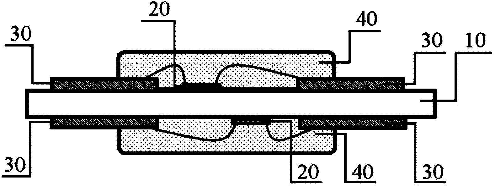
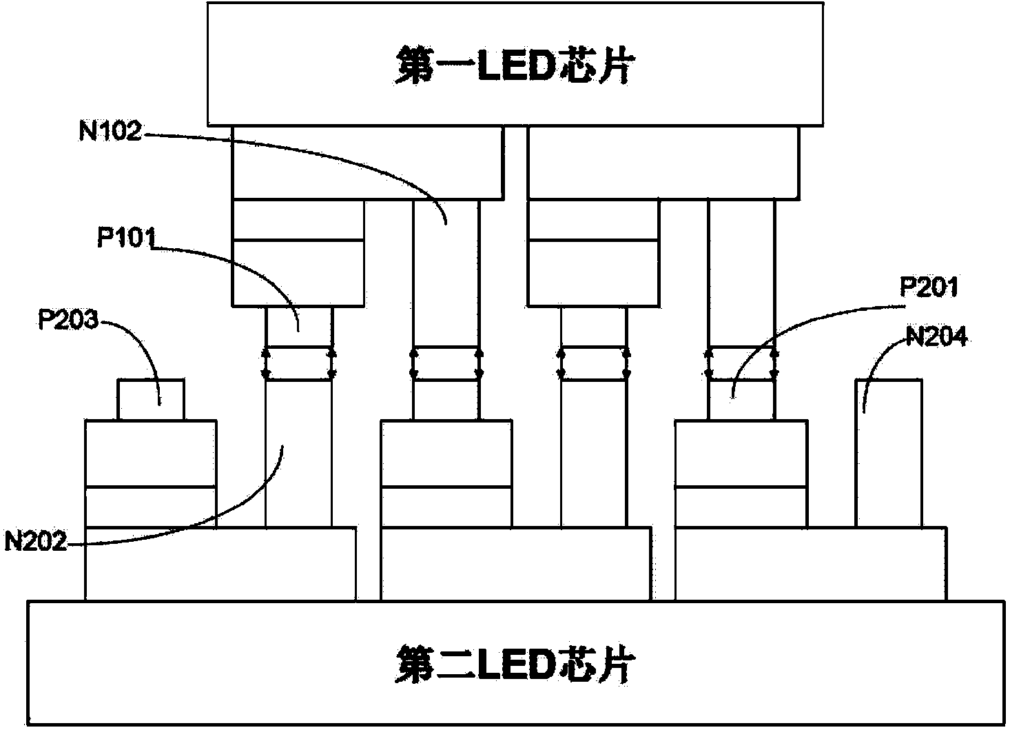
[0044] Figure 4 It is a structural schematic diagram of the LED device of the present invention, such as Figure 4 As shown, this embodiment discloses a three-dimensional light-emitting LED device, including a first direct-mount LED chip 100 (the LED chip located on the electrode lead-out metal sheet 300 in the figure) and a second direct-mount LED chip 100 that are oppositely arranged. Mounted LED chip 100 (the LED chip located under the electrode lead-out metal sheet 300 in the figure), the N electrode bonding layer of the first direct mount LED chip and the N electrode of the second direct mount LED chip There is an electrode lead-out metal sheet 300 electrically connected between the bonding layers (since its function is to lead out the N electrode of the LED, it can also be called the N electrode lead-out metal sheet), and the P electrode bond of the first direct mount LED chip There is an electrode lead-out metal sheet 300 electrically connected between the bonded laye...

Embodiment 2

[0058] like Figure 5 As shown, the difference between this embodiment and Embodiment 1 lies in that the shape of the light-converting substance material layer 200 is different.

[0059] In this embodiment, during the manufacturing process of the light conversion substance material layer 200, the three-dimensional light-emitting device manufactured by using a specially designed mold top mold has a light-emitting form of an LED light-emitting sphere, which realizes 360° full-angle light emission.

Embodiment 3

[0061] The only difference in this embodiment is that the manufacturing method of the three-dimensional light-emitting LED device is slightly different:

[0062] like Image 6 As shown, in this embodiment, after the direct mount LED chip 100 is fabricated, the light-converting material layer 200 is fabricated on its outer surface, and then bonded to the electrode lead-out metal sheet 300 .


PUM


Abstract

The invention belongs to the technical field of LEDs, and particularly discloses a three-dimensional luminous LED device and a manufacturing method thereof. The LED device comprises a first directly mounted LED chip and a second directly mounted LED chip, wherein the first directly mounted LED chip and the second directly mounted LED chip are arranged oppositely. An N electrode leading-out metal sheet is electrically connected between an N electrode bonding layer of the first directly mounted LED chip and an N electrode bonding layer of the second directly mounted LED chip, a P electrode leading-out metal sheet is electrically connected between a P electrode bonding layer of the first directly mounted LED chip and a P electrode bonding layer of the second directly mounted LED chip, and the outer surface of the first directly mounted LED chip and the outer surface of the second directly mounted LED chip are respectively provided with a light conversion material layer. The three-dimensional luminous LED device is large in light-emitting area and has the advantages of being good in heat dissipation performance, easy to manufacture and process, high in product yield and long in service life.

Description

technical field [0001] The invention belongs to the technical field of LEDs, and in particular relates to a three-dimensional light-emitting LED device and a manufacturing method thereof. Background technique [0002] Stereo-luminous LED lighting products have the advantages of almost 360-degree full-angle light, such as spherical, square and other shapes of bulbs and landscape lights, which can directly replace traditional incandescent lamps, fluorescent tubes, metal halide lamps, etc. to meet some household, Plaza, outdoor landscape lighting needs. At present, all single light sources on the market emit light on one side. To make a two-sided 360° light source, two single light sources need to be spliced ​​together, but the entire light source will be larger and take up more space. [0003] Such as figure 1 As shown, Chinese patent application number 201310123520.7 discloses an LED packaging structure, which adopts double-sided packaging of a front-mounted chip and a tran...

Claims


Application Information

Patent Timeline
Patent Type & Authority Applications(China)
IPC IPC(8): H01L33/48H01L33/50H01L33/00
CPCH01L33/48H01L25/0756H01L33/62H01L33/647H01L2933/0033
Inventor 万垂铭曾照明许朝军姜志荣肖国伟
Owner APT ELECTRONICS
Why Eureka
Try Eureka