

DC voltage-boosting chopper circuit
A chopper circuit, DC boost technology, applied in the direction of converting DC power input to DC power output, electrical components, adjusting electrical variables, etc., can solve the problem of inability to meet the requirements of power supply voltage, poor versatility, and inability to continuously adjust the output voltage range and other problems, to achieve the effect of wide adjustable range, small step and high precision
- Summary
- Abstract
- Description
- Claims
- Application Information
AI Technical Summary
Problems solved by technology
Method used
Image

Examples
Embodiment 1
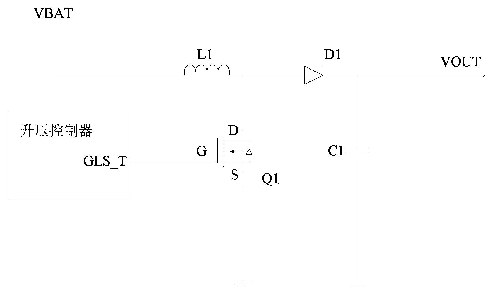
[0030] DC boost chopper circuit, including a boost inductor L1, a freewheeling diode D1, an output capacitor C1, a MOS switch Q1, a first resistor R1, a second resistor R2, a third resistor R3, a boost control device, a digital-to-analog converter DAC;
[0031] One end of the source drain of the MOS switch Q1 is grounded, and the other end is connected to the positive end of the freewheeling diode D1 and one end of the boost inductor L1;
[0032] The gate of the MOS switch Q1 is connected to the output terminal of the gate drive signal GLS_T of the boost controller;
[0033] The other end of the boost inductor L1 is connected to an external power supply VBAT;
[0034] The negative terminal of the freewheeling diode D1 is used as the boost voltage VOUT output terminal of the DC boost chopper circuit;
[0035] The output capacitor C1 is connected between the negative terminal of the freewheeling diode D1 and the ground;
[0036] The first resistor R1 and the second resistor R...
Embodiment 2
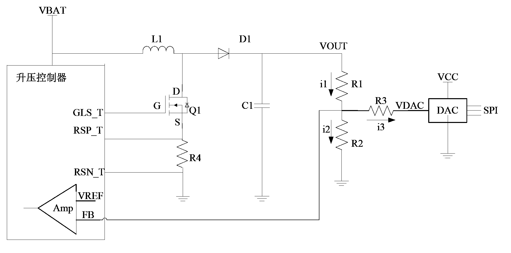
[0043] Based on Embodiment 1, the DC boost chopper circuit further includes a fourth resistor R4;
[0044] The source and drain of the MOS switch tube Q1 are grounded through the fourth resistor R4 at one end;
[0045] Both ends of the fourth resistor R4 are connected to two current sampling input terminals RSP_T and RSN_T of the boost controller, and are used to sample the source and drain current of the MOS switch tube Q1;
[0046] The boost controller controls and outputs the gate drive signal GLS_T according to the output of the comparator AMP and the source-drain current sampling of the MOS switch tube Q1, thereby stabilizing the boost voltage output by the negative terminal of the freewheeling diode D1 VOUT.
Embodiment 3
[0048] Based on the second embodiment, the MOS switch Q1 is an N-channel MOSFET (Metal-Oxide-Semiconductor Field-Effect Transistor, metal-oxide-semiconductor-field-effect transistor);
[0049] The source of the MOS switch Q1 is grounded through a fourth resistor, the drain is connected to the positive end of the freewheeling diode D1 and one end of the boost inductor L1, and the gate is connected to the gate drive signal GLS_T of the boost controller output.
PUM
| Property | Measurement | Unit |
|---|---|---|
| First resistor | aaaaa | aaaaa |
| Second resistor | aaaaa | aaaaa |
| Third resistor | aaaaa | aaaaa |
Abstract
Description
Claims
Application Information