A kind of preparation method of finfet structure

A wet etching and fin-shaped technology, which is applied in the field of FINFET structure preparation, can solve problems such as nitride removal defects, achieve the effect of avoiding incomplete removal, increasing the contact area, and the method is simple and easy

Active Publication Date: 2017-05-03
SHANGHAI HUALI MICROELECTRONICS CORP
View PDF7 Cites 0 Cited by
  • Summary
  • Abstract
  • Description
  • Claims
  • Application Information

AI Technical Summary

Problems solved by technology

However, the patent still has the problem of nitride removal defects

Method used


Image

  • A kind of preparation method of finfet structure
  • A kind of preparation method of finfet structure
  • A kind of preparation method of finfet structure

Examples


Embodiment Construction

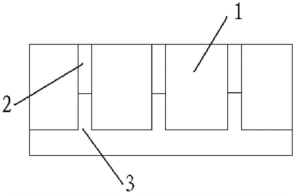
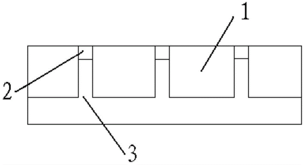
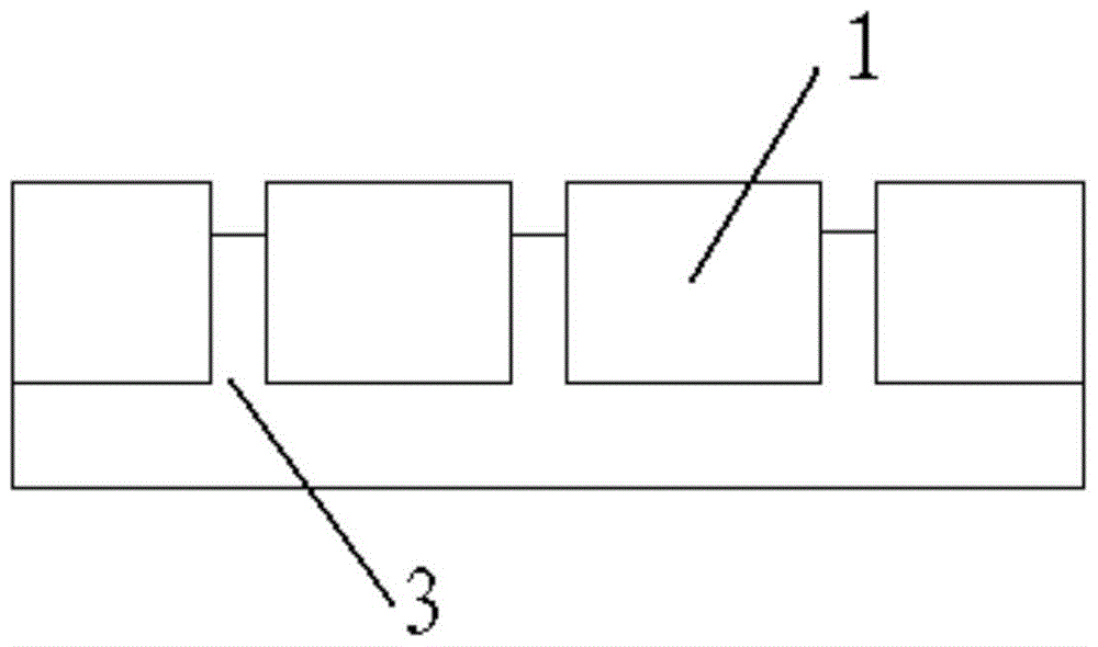
[0030] The invention provides a method for preparing a FINFET structure. After the conventional first step of CMP is completed, the grinding liquid with a low selectivity ratio is further used for grinding to reduce the thickness of silicon nitride, and finally make the silicon nitride reach an acceptable thickness. Meets the requirements for subsequent wet removal. Compared with the prior art, this method reduces the thickness of silicon nitride, and after a period of grinding, the width of exposed silicon nitride will also increase, which will be beneficial to wet cleaning. And because the rate of removal of silicon oxide by the low-selectivity slurry is greater than that of silicon nitride, after a period of grinding, the silicon nitride is in a raised state, which is more conducive to the removal of wet methods, and finally achieves the complete removal of silicon nitride. Effect.

[0031] The method of the present invention will be described in detail below in conjunctio...


PUM


Abstract

The invention provides a preparation method of an FINFET (fin-field effect transistor) structure. The preparation method comprises the steps of grinding silicon oxide 1 on silicon nitride 2; continuously grinding a certain amount of silicon oxide 1 and silicon nitride 2 with low-selection-ratio grinding fluid so as to reduce the thickness of the silicon nitride 2; wet etching to remove the silicon nitride; wet etching to remove part of silicon oxide 1 for forming the FinFET structure. The technical scheme of the invention is easy and feasible, twice CMP processes are utilized for reducing thickness of the silicon nitride and increasing the width of the silicon nitride, namely, the contact area of the silicon nitride and medicament is increased, a wet method is facilitated to remove the silicon nitride and finally remove the silicon nitride completely, so that the consequence of incomplete removal of the silicon nitride is avoided.

Description

technical field [0001] The invention relates to the field of semiconductor manufacturing, in particular to a method for preparing a FINFET structure. Background technique [0002] The FinFET is called a Fin Field-Effect Transistor (Fin Field-Effect Transistor; FinFET) and is a new complementary metal oxide semiconductor (CMOS) transistor. Fin means fish fin, and FinFET is named according to the similarity between the shape of the transistor and the fish fin. [0003] At present, the existing technology forms FinFET by CMP. After the first step of conventional STI (shallow trench isolation)-CMP is completed, the second step uses dry etch (dry etching) to etch a certain amount of oxide (oxidation) In the third step, H3PO4 is used to remove Nitride (nitride) on the active region, and in the fourth step, a certain amount of oxide is etched away by wet etch (wet etching), finally forming a FinFET structure. [0004] In this integration scheme, when Nitride remove (nitride remov...

Claims


Application Information

Patent Timeline
Patent Type & Authority Patents(China)
IPC IPC(8): H01L21/336H01L21/306
CPCH01L21/31056H01L21/31111H01L29/66795
Inventor 丁弋陈锟朱也方李芳王从刚
Owner SHANGHAI HUALI MICROELECTRONICS CORP
Why Eureka
Try Eureka