Package structure and manufacturing method thereof

A technology of packaging structure and manufacturing method, which is applied in the direction of multilayer circuit manufacturing, semiconductor/solid-state device manufacturing, electrical components, etc., can solve the problems such as the inability of the first insulating layer to be thinned and the overall thickness of the packaging structure to be thinned.

Inactive Publication Date: 2014-06-18
HONGQISHENG PRECISION ELECTRONICS (QINHUANGDAO) CO LTD +1
View PDF4 Cites 5 Cited by
  • Summary
  • Abstract
  • Description
  • Claims
  • Application Information

AI Technical Summary

Problems solved by technology

However, in the packaging structure made by the above method, in order to accommodate the electronic components in the through holes of the first insulating layer, the thickness of the first insulating layer must be set to be equivalent

Method used


Image

  • Package structure and manufacturing method thereof
  • Package structure and manufacturing method thereof
  • Package structure and manufacturing method thereof

Examples


Embodiment Construction

[0020] The encapsulation structure provided by the technical solution and the manufacturing method of the encapsulation structure will be further described in detail below with reference to the drawings and embodiments.

[0021] The manufacturing method of the packaging structure provided by the embodiment of the technical solution includes the following steps:

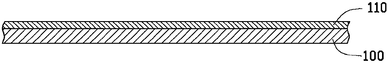
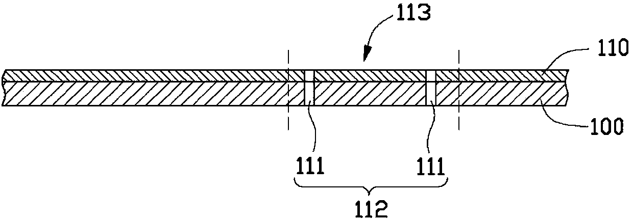
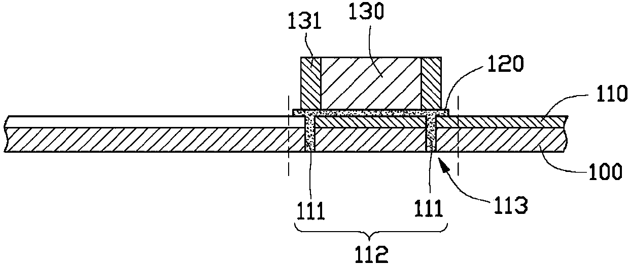
[0022] For a first step, see figure 1 , providing a carrier board 100 and a first copper foil 110 laminated with the carrier board 100 .

[0023] In this embodiment, both the first copper foil 110 and the carrier board 100 are rectangular and have the same size. The thickness of the first copper foil 110 is the commonly used thickness of copper foil in circuit board manufacturing, preferably 9 microns-35 microns. The carrying plate 100 plays a role of supporting the first copper foil 110, and the carrying plate 100 can be a metal plate such as a copper plate, an aluminum plate, a steel plate, etc., or can be a coppe...


PUM


Abstract

Disclosed is a manufacturing method of a package structure. The method includes the following steps: providing a first copper foil which includes at least one surface-mount area and fixing at least one element on a surface-mount area through a non-conductive electric-glue layer; providing an inner-layer core plate which is provided with at least one second through hole; and providing a first adhesive sheet, a second adhesive sheet and a second copper foil, wherein at least one forth through hole is formed in the first adhesive sheet and each forth through hole is corresponding to a second through hole; sequentially laminating and thermopressing a bearing plate, the first copper foil, the first adhesive sheet, the inner-layer core plate, the second adhesive sheet and the second copper foil so as to make the elements pass through the forth through holes and accommodated in the second through holes; and then manufacturing the first copper foil and the second copper foil so as to form a first external-layer conductive circuit layer and a second external-layer conductive circuit layer so that a package structure is formed. The invention also provides the package structure manufactured through the above-mentioned manufacturing method.

Description

technical field [0001] The invention relates to circuit board manufacturing technology, in particular to a packaging structure and a manufacturing method thereof. Background technique [0002] One of the manufacturing methods of the packaging structure commonly used in the industry is: providing a copper-clad core board, the copper-clad core board includes a first conductive circuit layer, a first insulating layer and a second conductive circuit layer; Form a through hole through the copper clad core board; provide an electronic component, a first outer conductive layer, a second insulating layer, a third insulating layer and a second outer conductive layer, wherein the electronic component The height of the device is equivalent to the thickness of the first insulating layer of the copper clad core board, the size of the electronic component is smaller than the size of the through hole, and the second insulating layer and the third insulating layer have semi-cured properties...

Claims


Application Information

Patent Timeline
IPC IPC(8): H01L23/498H01L23/31H01L21/60H01L21/56H05K3/46
CPCH01L2924/0002
Inventor 李泰求
Owner HONGQISHENG PRECISION ELECTRONICS (QINHUANGDAO) CO LTD
Why Eureka
Try Eureka