Photovoltaic and luminescence characterization methods for one-dimensional nanostructures and three-dimensional micro-regions

A nanostructure and photovoltaic technology, applied in materials excitation analysis and other directions, can solve the problems of photovoltaics that cannot measure three-dimensional directions, and cannot be synchronously characterized.

Active Publication Date: 2016-03-23
HUNAN UNIV
View PDF6 Cites 0 Cited by
  • Summary
  • Abstract
  • Description
  • Claims
  • Application Information

AI Technical Summary

Problems solved by technology

[0004] The present invention provides a system and method for characterization of photovoltaic and luminescence in three-dimensional direction micro-regions of one-dimensional nanostructures. At the same time, it also overcomes the problem that the existing technology can only measure the photovoltaic signal generated in a certain dimension, but cannot measure the photovoltaic in three dimensions.

Method used


Image

  • Photovoltaic and luminescence characterization methods for one-dimensional nanostructures and three-dimensional micro-regions
  • Photovoltaic and luminescence characterization methods for one-dimensional nanostructures and three-dimensional micro-regions
  • Photovoltaic and luminescence characterization methods for one-dimensional nanostructures and three-dimensional micro-regions

Examples


Embodiment 1

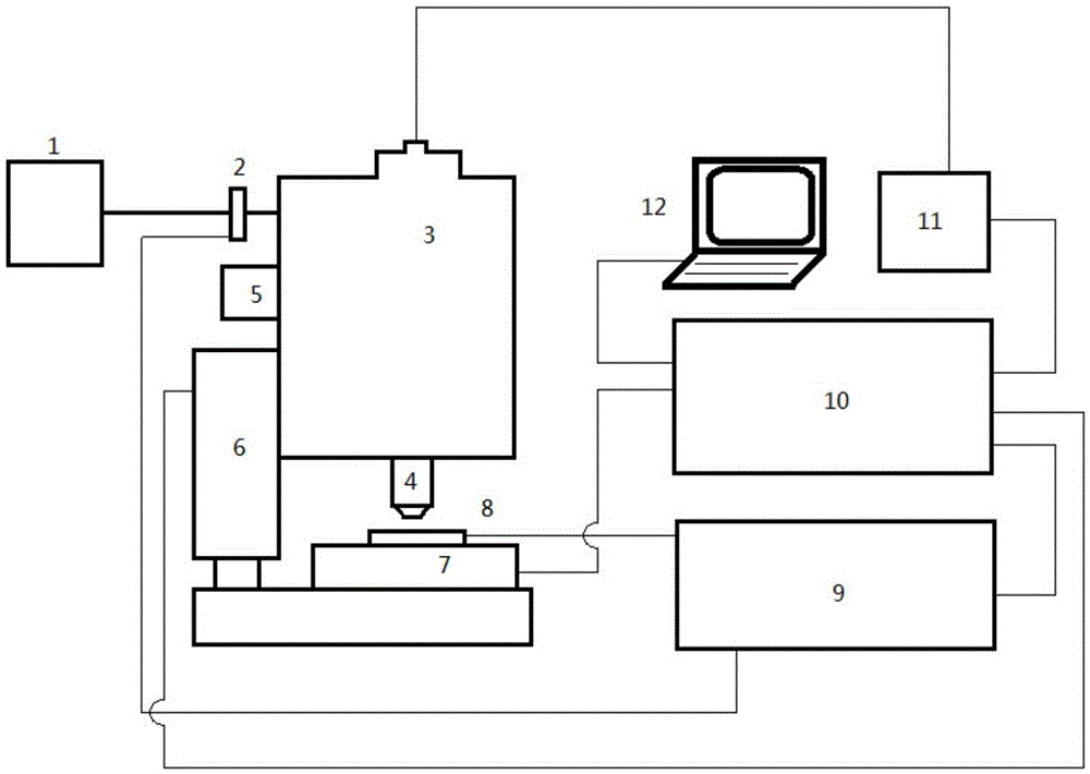
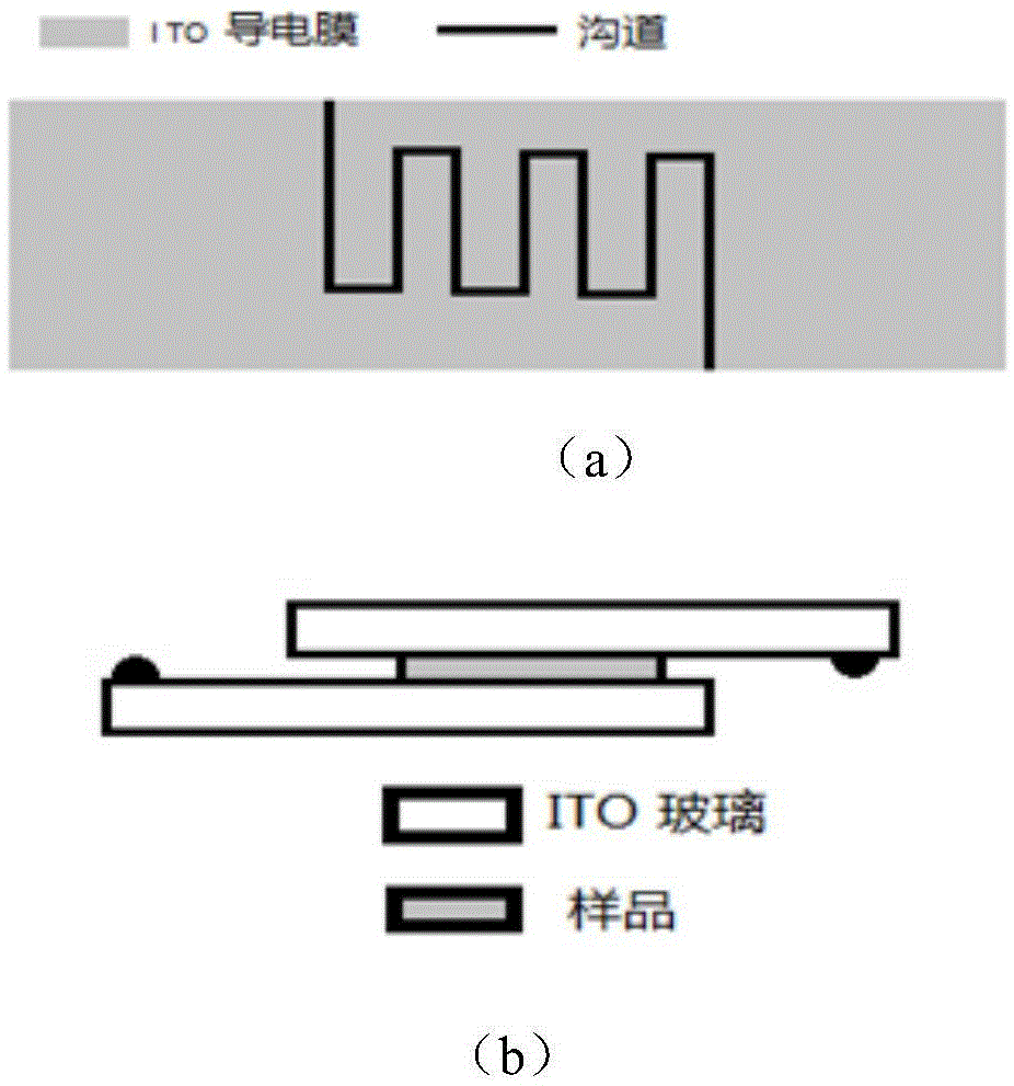
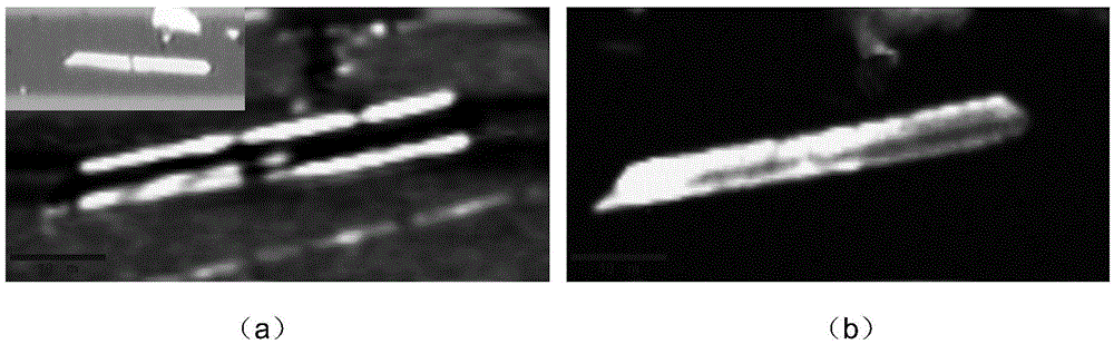
[0071] The CdS nanobelts are dispersed in the channel electrode, so that the nanobelts are parallel or perpendicular to the electrodes; the sandwich structure electrode is that the thickness direction of the nanobelt is perpendicular to the two electrodes, and the two ends of the channel electrode or the two electrodes of the sandwich structure are connected to the lock-in amplifier. 9 Connect with coaxial cable. The laser light emitted by the 488nm argon ion laser 1 is modulated by the chopper 2 and then coupled into the optical fiber, and introduced into the confocal microscope system. The laser light is focused by the objective lens 4 to the CdS nanobelts dispersed on the electrode 8. The photovoltaic signal has the same modulation frequency as the chopper, and the lock-in amplifier can amplify the photovoltaic signal generated by the CdS nanobelt after being synchronized by the chopper. The output photovoltaic signal of the lock-in amplifier is input to the confocal micros...

Embodiment 2

[0077] The nanowires are dispersed within the channel electrode so that the nanowires are parallel to the electrode or perpendicular to the electrode. Both ends of the channel electrode are connected to the lock-in amplifier 9 by a coaxial cable. The laser light emitted by the 488nm argon ion laser 1 is modulated by the chopper 2 and then coupled into the optical fiber and introduced into the confocal microscope system 3. The laser light is focused by the objective lens 4 to the nanowires scattered on the electrode 8, and the photovoltaic generated by the excitation of the nanowires The signal has the same modulation frequency as the chopper, and the lock-in amplifier can amplify the photovoltaic signal generated by the nanowire after being synchronized by the chopper. The photovoltaic signal output by the lock-in amplifier is input to the confocal microscope system controller 10 through a coaxial cable. The luminescent signals simultaneously generated by the nanowires pass t...


PUM

PropertyMeasurementUnit
widthaaaaaaaaaa
depthaaaaaaaaaa
thicknessaaaaaaaaaa

Abstract

The invention discloses a one-dimensional nano structure three-dimensional direction microcell photovoltaic and lighting representing system and method. A one-dimensional nano structure is arranged in a channel electrode; an electrode does not need to be in ohmic contact with the one-dimensional nano structure; a tested nano wire / belt is moved through a micro probe to change the position of the nano wire / belt so as to enable the nano wire / belt to be parallel to or perpendicular to the electrode; photovoltaic generated when photogenerated charges are separated along the width or length direction is measured; photovoltaic generated when the photogenerated charges are separated along the height direction is measured by using a sandwich structure; meanwhile, with the combination of a coaxially triggered confocal microscopy, the size of a triggered light spot is focused to the limited diffraction size of light, and the synchronous scanning imaging measurement on the microcell photovoltaic and optical response of the resolution at the limited light diffraction is achieved.

Description

technical field [0001] The invention belongs to the photoelectric measurement technology of semiconductor nanostructures, and in particular relates to a system and method for characterizing photovoltaic and luminescence of one-dimensional nanostructures in three-dimension micro-area. Background technique [0002] Luminescence and photovoltaics are two fundamental physical processes that occur in semiconductor materials under the excitation of bandgap light. Luminescence is generated by the recombination of photo-generated electron-hole pairs, while photovoltaics are generated by the spatial separation of photo-generated electron-hole pairs. Typically, the two are competing processes. Therefore, the simultaneous characterization of luminescence and photovoltaic signals will play a positive role in the study and correct understanding of fundamental photophysical processes. [0003] Due to their good optical and electrical properties, semiconductor one-dimensional nanostructu...

Claims


Application Information

Patent Timeline
Patent Type & Authority Patents(China)
IPC IPC(8): G01N21/63
Inventor 张清林潘安练
Owner HUNAN UNIV
Why Eureka
Try Eureka