

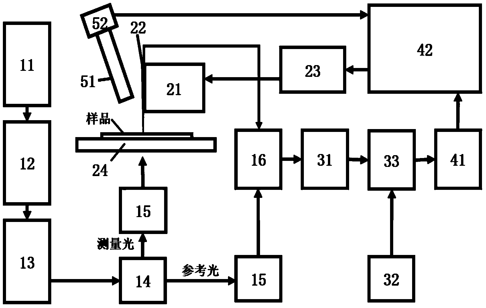
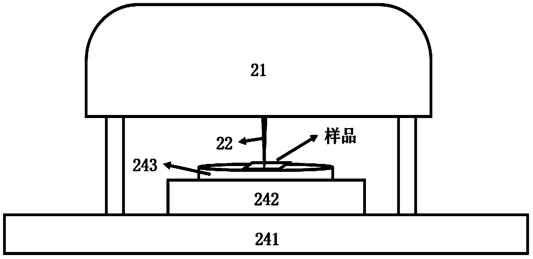
Device for measuring nano-scale light field phase distribution
A nanoscale and measurement device technology, applied in the field of nano-optics and nano-photonics measurement, can solve the problems of inability to measure phase distribution and achieve the effect of synchronous scanning imaging measurement
- Summary
- Abstract
- Description
- Claims
- Application Information
AI Technical Summary
Problems solved by technology
Method used
Image


Examples
example 1
[0061] Example 1. Control of in-plane light field by surface plasmon devices
[0062] Surface plasmon polaritons (SPPs) are electromagnetic oscillations coupled with charge density fluctuations excited on the metal-dielectric interface. They have the characteristics of near-field enhancement, surface confinement, and short wavelength. play an important role in the research. Usually, the wavevector of SPPs and the wavevector of light do not match, so SPPs can only be excited under certain incident angles and polarization states.
[0063] This example introduces an in-plane focusing arc structure, which is designed using the principle of SPP phase interference, and can realize directional excitation and focusing of left and right circularly polarized light.
[0064] S1. Coating a layer of metal film on the glass substrate, the metal material can be gold or silver, and the thickness of the film is about 50nm, so that the evanescent field can pass through the metal film from the ...
example 2
[0068] Example 2. Research on the distribution characteristics and propagation modes of the optical field in the micro-nano optical waveguide
[0069] S1. Coating a layer of gold film on the glass substrate, the film thickness is less than 100nm to ensure light transmittance; grow 500nm photoresist on the gold film, after exposure and corrosion, cure a 3 micron wide optical waveguide on the surface;
[0070] S2. The excitation light source is a semiconductor laser with a wavelength of 532nm. After beam shaping and focusing, a spot with a diameter of about 20 microns is irradiated at the position of the waveguide on the sample plane;
[0071] S3. When the SPP excited on the surface propagates, when encountering the waveguide structure, light will be coupled into the waveguide and continue to propagate; when the incident angle is changed, different light field modes can be excited in the waveguide.
[0072] S4. Combined with the law of phase distribution and amplitude distributi...
example 3
[0074] Example 3. Research on phase modulation of light field by metal nanoantenna array
[0075] When the beam passes through the regularly arranged nano-metal array, the phase of the transmitted beam will be delayed to different degrees due to the coupling and interaction between the electric field and the free electrons in the metal. The amount of retardation depends on the size, shape and arrangement of the nanorods. After mastering this rule, the nano-antenna array can be arranged artificially to modulate the phase of the incident plane beam to produce the desired wavefront distribution.
[0076] S1, using EBL and lift-off methods to fabricate gold nanorod arrays on glass substrates;
[0077] S2. The arrangement direction of the gold nanorods in the array changes regularly according to the modulation requirement. The rods are 50nm wide, 200nm long, and 40nm high, and the distance between two adjacent rods is 400nm.
[0078] S3. The excitation light source adopts a He-N...
PUM
 Abstract
Description
Claims
Application Information