

Projection type planar waveguide helmet-mounted displayer
A helmet-mounted display and planar waveguide technology, applied in light guides, instruments, optics, etc., can solve the problems of large display size, reduce stray light, reduce design difficulty, and expand the observation field of view
- Summary
- Abstract
- Description
- Claims
- Application Information
AI Technical Summary
Problems solved by technology
Method used
Image

Examples
Embodiment 1
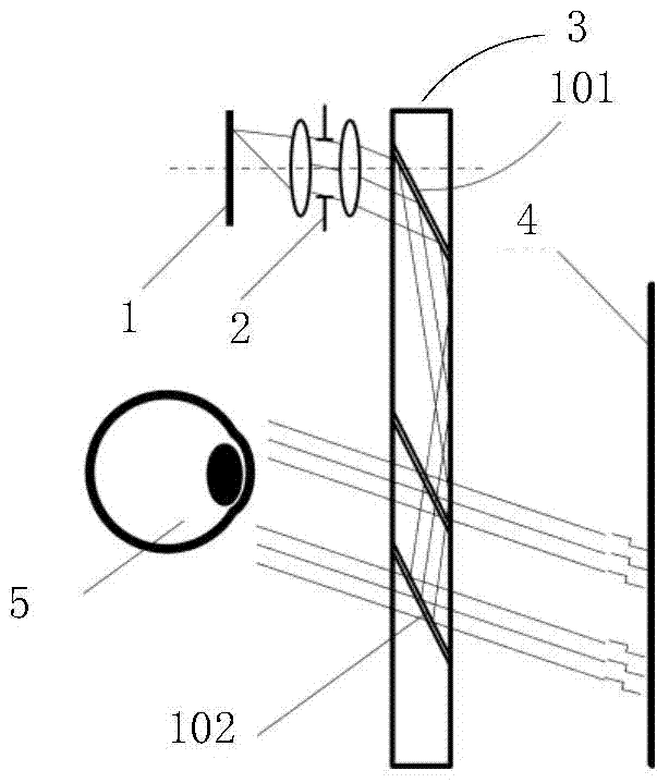
[0050] Such as figure 2 As shown, the structure of the planar waveguide in this embodiment is a rectangular waveguide structure, which specifically includes an optical coupling end 101 and an optical coupling end 102. The optical coupling end 101 of the planar waveguide is a mirror, and the optical coupling end 102 of the planar waveguide 102 is more than two half-mirrors placed in parallel, and the angle between the half-mirror and the reflective surface of the planar waveguide is greater than 15° and less than 40°.
[0051] In Embodiment 1, a reflector is used to ensure that the light entering the planar waveguide satisfies the condition of total reflection of the light in the planar waveguide after being reflected by it, and the reflector is used as the optical coupling end to ensure the overall rectangular shape of the planar waveguide, which is convenient for installation. The light emitted by the display 1 enters the planar waveguide 3 after being imaged by the projecti...
Embodiment 2
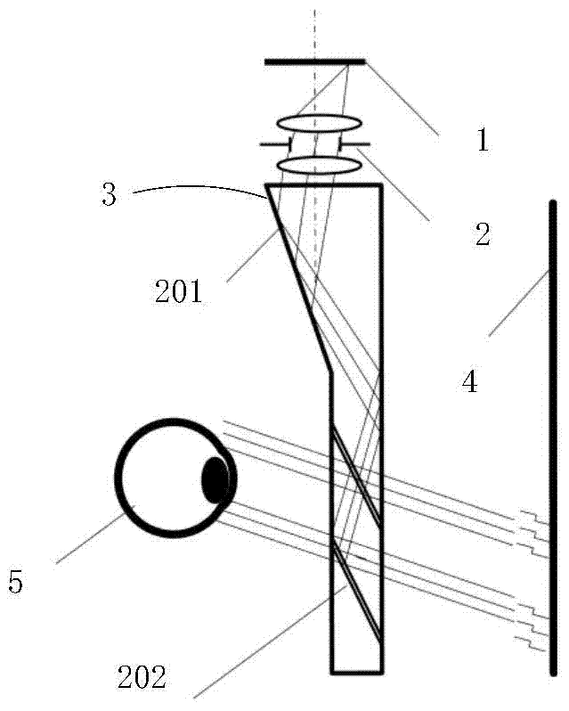
[0053] Such as image 3 As shown, the structure of the planar waveguide 3 in this embodiment is an irregular structure, and the reflection area where the light enters the planar waveguide 3 for the first reflection is a slope, and the slope serves as the optical coupling end 201 of the planar waveguide 3, and the slope The surface is coated with a reflective film, and the slope needs to ensure that the light entering the planar waveguide meets the conditions of total reflection of the light in the planar waveguide after being reflected by it. Using this structural form reduces the link of system glueing and processing, and is easy to process. After the light is incident on the planar waveguide 3 and reaches the optical coupling end 201, the light is reflected and is limited to propagate in the planar waveguide 3, and the light after entering the planar waveguide 3 The optical path is the same as that in Embodiment 1.
Embodiment 3
[0055] Such as Figure 4 As shown, in this embodiment, the reflective surface where light enters the planar waveguide 3 for the first reflection is a holographic or diffractive surface. The final photosensitive coating or a microstructure surface capable of deflecting light is formed by photolithography or other techniques. Using this structure as an optical coupling port can simplify the optical projection system. The light enters the planar waveguide 3 and reaches the optical coupling end 301 for reflection and is restricted to propagate in the planar waveguide 3 . The light path after entering the planar waveguide 3 is the same as that of the first embodiment.
PUM
| Property | Measurement | Unit |
|---|---|---|
| Angle | aaaaa | aaaaa |
Abstract
Description
Claims
Application Information