Standard cell design method resistant to single-particle latch-up effect

A standard cell and latch-up effect technology, applied in computing, special data processing applications, instruments, etc., can solve problems such as limiting the working speed and scale of radiation-resistant devices, increasing cell area, parasitic capacitance, and reducing circuit speed, etc., to achieve small Effects of layout design modification, increased flexibility, and mitigation effects

Active Publication Date: 2014-06-25
XIAN INSTITUE OF SPACE RADIO TECH
View PDF4 Cites 8 Cited by
  • Summary
  • Abstract
  • Description
  • Claims
  • Application Information

AI Technical Summary

Problems solved by technology

Under the bombardment of heavy ions, a single event current will appear in the p-n junction of the well / substrate, causing a voltage drop in the well, which will cause the parasitic transistor in the latch structure (NPNP) to turn on, forming a positive feedback loop, and continuously increasing the current , eventually causing the device to be burned
[0003] At present, domestic anti-single event latch-up design and reinforcement for CMOS integrated circuits are mostly oriented to 0.18um CMOS process and adopt guard ring reinforcement method. Firstly, the process size limits the working speed and scale of radiation-resistant devices, and secondly, the guard ring structure will cause layout layout. It is more difficult, greatly increasing the area of ​​the unit, parasitic capacitance, and reducing the speed of the circuit

Method used


Image

  • Standard cell design method resistant to single-particle latch-up effect
  • Standard cell design method resistant to single-particle latch-up effect
  • Standard cell design method resistant to single-particle latch-up effect

Examples


Embodiment Construction

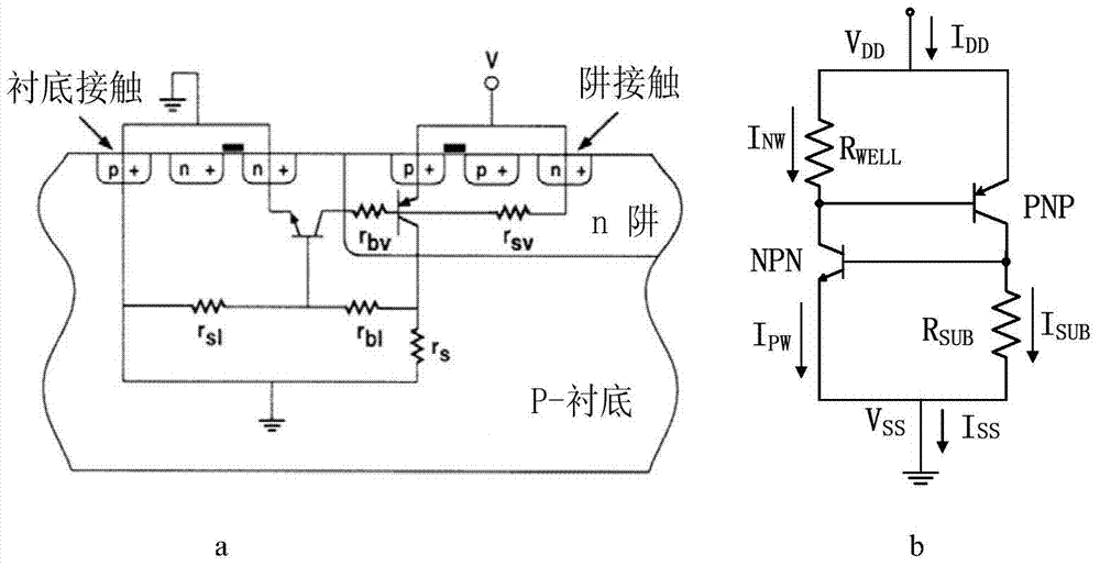
[0025] Combined with the mechanism analysis of single event latch-up effect, the basic principle to avoid latch-up effect is:

[0026] (1) Reduce well / substrate parasitic resistance. When a single event current (IWELL) occurs in the well / substrate p-n junction, reducing the well resistance (RWELL) is equivalent to reducing the voltage drop between the emitter and base of the vertical parasitic PNP transistor in the well, thereby reducing the trigger Risk of parasitic PNP transistor turning on;

[0027] (2) Destroy the characteristics of the parasitic bipolar transistor and reduce the current gain of the transistor. Reducing the gain of the parasitic transistor in the latch structure is equivalent to reducing the feedback loop current gain of the two parasitic transistors, so as to avoid continuous increase of the positive feedback loop current in the latch structure.

[0028] Aiming at the damage mechanism of spatial single event latch-up effect to CMOS integrated circuits, ...


PUM


Abstract

A standard cell design method resistant to the single-particle latch-up effect comprises the steps that (1) trap contact protecting regions are arranged in a standard cell layout, namely areas in contact connection with traps in the standard cell layout and stretch to two sides of a transistor active area are arranged into the protecting regions, and multiple contact holes are formed in the trap contact protecting regions; (2) separation distances of the trap contact protecting regions are reduced, and the biggest separation distance (dWC) of the trap contact protecting regions is not more than 4 microns; (3) the separation distance between an NMOS and a PMOS active area is increased, and the separation distance between the NMOS and the PMOS active area is not less than 0.69 micron; (4) the distance between each trap contact protecting region and an MOS transistor source electrode is reduced, the width of a first metal layer, the width of a second metal layer and the width of a third metal layer are respectively 0.4 micron according to the design rule of the SMIC013MMRF technology, and the height of an adopted unit is 4.0 microns equivalent to the pitch widths of 10 metal layers. The method achieves reinforcing of resistance to the single-particle latch-up effect, and is low in cost, easy to implement and high in reliability.

Description

technical field [0001] The invention relates to a standard unit design method for resisting single-event latch-up effect, which belongs to CMOS integrated circuit space single-event effect protection technology. Background technique [0002] The spatial single event latch-up effect mainly appears in CMOS integrated circuits, which is caused by its internal parasitic n-p-n-p structure. The parasitic latch structure under the CMOS process is as figure 1 shown. Under the bombardment of heavy ions, a single event current will appear in the p-n junction of the well / substrate, causing a voltage drop in the well, which will cause the parasitic transistor in the latch structure (NPNP) to turn on, forming a positive feedback loop, and continuously increasing the current , eventually causing the device to be burned. [0003] At present, domestic anti-single event latch-up design and reinforcement for CMOS integrated circuits are mostly oriented to 0.18um CMOS process and adopt guar...

Claims


Application Information

Patent Timeline
Patent Type & Authority Applications(China)
IPC IPC(8): G06F17/50
Inventor 周国昌巨艇赖晓玲王轩张健
Owner XIAN INSTITUE OF SPACE RADIO TECH
Why Eureka
Try Eureka