Display panel and display device thereof

A technology for display panels and display devices, applied in static indicators, instruments, electrical components, etc., can solve problems such as resolution improvement, and achieve the effects of low power consumption, improved image resolution, and large color coverage.

Inactive Publication Date: 2014-06-25
AU OPTRONICS CORP
View PDF0 Cites 29 Cited by
  • Summary
  • Abstract
  • Description
  • Claims
  • Application Information

AI Technical Summary

Problems solved by technology

However, this design also has a certain limit in terms of resolution improvement

Method used


Image

  • Display panel and display device thereof
  • Display panel and display device thereof
  • Display panel and display device thereof

Examples


Embodiment Construction

[0030] In order to make the technical content disclosed in this application more detailed and complete, reference may be made to the drawings and the following various specific embodiments of the present invention, and the same symbols in the drawings represent the same or similar components. However, those skilled in the art should understand that the examples provided below are not intended to limit the scope of the present invention. In addition, the drawings are only for schematic illustration and are not drawn according to their original scale.

[0031] The specific implementation manners of various aspects of the present invention will be further described in detail below with reference to the accompanying drawings.

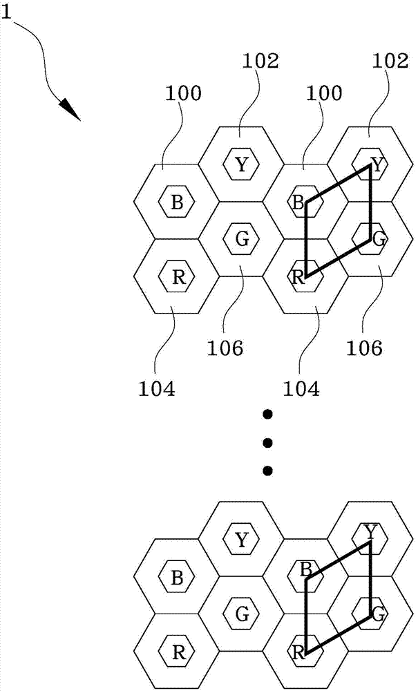
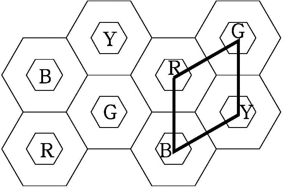
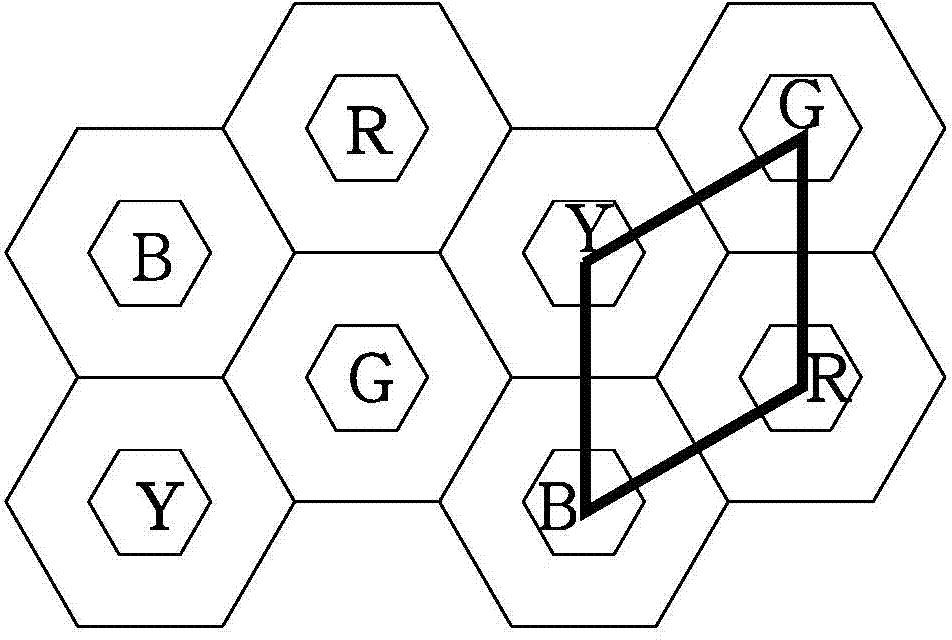
[0032] figure 1 A schematic diagram of pixel arrangement of a display panel according to an embodiment of the present invention is shown. The display panel of the present invention has a pixel array (pixel array). The pixel array includes a plurality of ...


PUM


Abstract

The invention provides a display panel and a display device thereof. The display panel is provided with a pixel array. The pixel array comprises multiple pixel units, each pixel unit is formed by two first sub pixels, two second sub pixels, two third sub pixels and two fourth sub pixels, and any two adjacent sub pixels are of different colors. The connecting lines of the centers of the adjacent first sub pixels, the centers of the adjacent second sub pixels, the centers of the adjacent third sub pixels and the centers of the adjacent fourth sub pixels form a non-rectangular parallelogram. Compared with the prior art, the display panel and the display device thereof can reduce the number of the sub pixels of each original pixel from three to two to reduce the area of pixel layout of the pixels, and image resolution in display can be improved. In addition, sub pixel design of RGBY four colors is adopted by the pixel units of the display panel and the display device thereof, and power consumption is lowered by being compared with sub pixel design of RGB three-primary colors.

Description

technical field [0001] The invention relates to the fields of semiconductor technology and organic electroluminescent display technology, in particular to a display panel with a novel pixel arrangement structure and a display device thereof. Background technique [0002] Organic light emitting diodes (Organic Light Emitting Diode, OLED) can be divided into passive matrix driving (Passive Matrix OLED, PMOLED) and active matrix driving (Active Matrix OLED, AMOLED) according to the driving method. PMOLED is that when the data is not written, the light-emitting diode does not emit light; only when the data is written, the light-emitting diode emits light. This driving method is simple in structure, low in cost, easy to design, and is mainly suitable for small and medium-sized displays. In AMOLED, each pixel has a capacitor to store data, so that each pixel maintains a light-emitting state. Since the power consumption of AMOLED is significantly lower than that of PMOLED, and it...

Claims


Application Information

Patent Timeline
Patent Type & Authority Applications(China)
IPC IPC(8): H01L27/32G09G3/32G09G3/3225
Inventor 沈仕旻李孟庭
Owner AU OPTRONICS CORP
Why Eureka
Try Eureka