Display device and method for making same

a technology for display devices and display panels, applied in the direction of sustainable manufacturing/processing, instruments, final product manufacturing, etc., can solve the problems of pixel density limitation, not yet effectively solved, and degradation problems

Active Publication Date: 2019-01-10
HON HAI PRECISION IND CO LTD
View PDF0 Cites 9 Cited by
  • Summary
  • Abstract
  • Description
  • Claims
  • Application Information

AI Technical Summary

Problems solved by technology

However, the blue sub-pixels in OLED may have degradation problems, which have not yet been effectively solved.
H

Method used


Image

  • Display device and method for making same
  • Display device and method for making same
  • Display device and method for making same

Examples


first embodiment

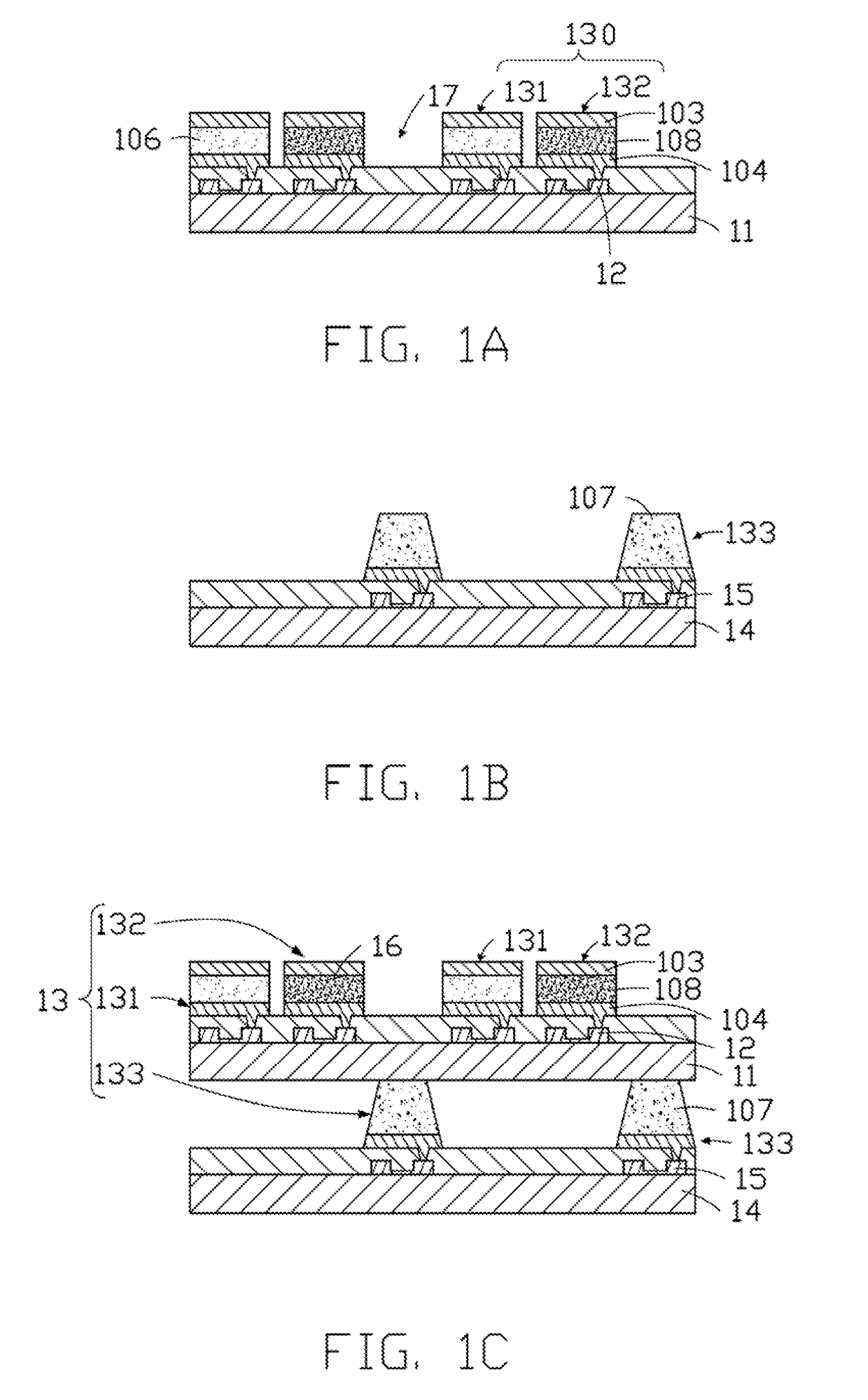
[0011]As shown in FIG. 1A through FIG. 1E, a display device 100 comprises a plurality of organic light emitting diodes (OLEDs) and a plurality of micro light emitting diodes (micro-LEDs). The display device 100 is a hybrid display device. In this embodiment, a size of each Micro-LED is less than 50×50 μm. A method for making the display device 100 comprises the following steps.

[0012]Step 1: as shown in FIG. 1A, a first substrate 11 is provided and a plurality of first light emitting elements 106 are provided on the first substrate 11. The first light emitting elements 106 are OLEDs.

[0013]In this embodiment, each first light emitting element 106 defines a pixel, the first light emitting elements 106 define a first pixel array on the first substrate 11.

[0014]In this embodiment, the first pixel array comprises a plurality of first sub-pixels 131 and a plurality of second sub-pixels 132. The first sub-pixels 131 and the second sub-pixels 132 emit light of different colors. In this embod...

second embodiment

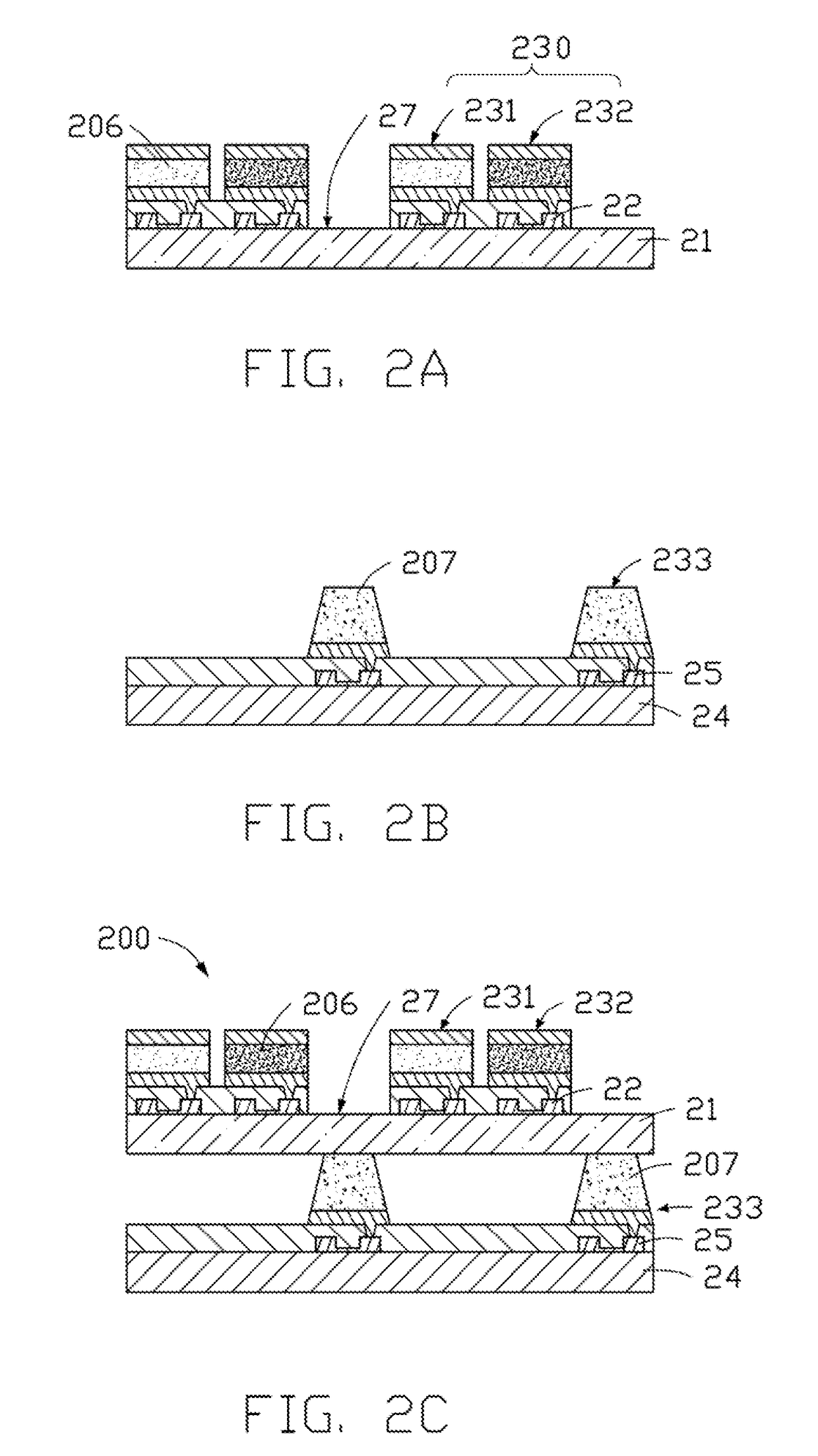
[0044]As shown in FIG. 2A through FIG. 2C, a display device 200 comprises a plurality of OLEDs and a plurality of micro-LEDs. The display device 200 is a hybrid display device. A method for making the display device 200 comprises the following steps.

[0045]Step 1: as shown in FIG. 2A, a first substrate 21 is provided, and a plurality of first light emitting elements 206 are provided on the first substrate 21. The first light emitting elements 206 are OLEDs.

[0046]In this embodiment, each first light emitting element 206 defines a pixel, and the first light emitting elements 206 define a first pixel array on the first substrate 21.

[0047]In this embodiment, the first pixel array comprises a plurality of first sub-pixels 131 and a plurality of second sub-pixels 232. The first sub-pixels 231 and the second sub-pixels 232 emit light of different colors. In this embodiment, the first sub-pixels 231 emit red light and the second sub-pixels 232 emit green light.

[0048]A plurality of first thin...

third embodiment

[0062]As shown in FIGS. 3A through 3C, a display device 300 comprises a plurality of OLEDs and a plurality of Micro-LEDs. The display device 300 is a hybrid display device. A method for making the display device 300 comprises the following.

[0063]Step 1: As shown in FIG. 3A, a first substrate 31 is provided, and a plurality of first light emitting elements 306 are provided on the first substrate 31. The first light emitting elements 306 are Micro-LEDs.

[0064]In this embodiment, each first light emitting element 306 defines a pixel, and the plurality of first light emitting elements 306 define a first pixel array on the first substrate 31.

[0065]In this embodiment, the first pixel array comprises a plurality of first sub-pixels 131 and a plurality of second sub-pixels 332, the first sub-pixels 331 and the second sub-pixels 332 emit light of different color. In this embodiment, the first sub-pixels 331 emit green light and the second sub-pixels 332 emit blue light.

[0066]A plurality of fi...


PUM


Abstract

A display device comprised of OLEDs and micro LEDs which allows for blue light degradation of the OLEDs includes a first substrate and a second substrate in a double-decked configuration. First light emitting elements are located and spaced on the first substrate and second light emitting elements are located and spaced on the second substrate, the light emitting elements on the lower deck being staggered so as not to be hidden by the light emitting elements on the upper deck. The upper deck has openings (or is transparent) therein to allow egress of light from the light emitting elements of the lower deck. The display device provides a solution for uneven display cause by degradation of pixels.

Description

FIELD[0001]The subject matter herein generally relates to a display panel and a method for making the display panel.BACKGROUND[0002]Organic light-emitting diode (OLED) has advantages of wide color range, thinness, and power efficiency. However, the blue sub-pixels in OLED may have degradation problems, which have not yet been effectively solved. The conventional processing method is to increase area of the blue sub-pixel, to ensure the display effect and prolong the life of the display device. However, in this method, the blue sub-pixels need to occupy a large area, which leads to a limit at pixel density.[0003]Therefore, there is room for improvement in the art.BRIEF DESCRIPTION OF THE DRAWINGS[0004]Implementations of the present technology will now be described, by way of example only, with reference to the attached figures.[0005]FIG. 1A through FIG. 1E are cross-sectional views showing a method for making a display according to a first embodiment of the present disclosure.[0006]F...

Claims


Application Information

Patent Timeline
IPC IPC(8): H01L27/32H01L51/52H01L51/50H01L51/00H01L51/56
CPCH01L27/3218H01L51/5206H01L51/5221H01L27/3262H01L51/0097H01L51/56H01L51/5036H10K59/35H10K59/12H10K71/80H10K59/1201H01L25/0753Y02E10/549Y02P70/50H10K59/00H10K50/80G09G2300/0452H01L25/162H01L25/075H10K59/353H10K50/81H10K50/82H10K50/115H10K50/125H10K59/1213H10K71/00H10K77/111
Inventor LIN, CHANG-TINGCHANG, WEI-CHIHCHEN, YING-CHIEHLAI, CHUNG-WENHUANG, CHUN-CHIEHWANG, WEI-LILU, PO-YICHEN, JEN-JIEWU, I-WEI
Owner HON HAI PRECISION IND CO LTD
Why Eureka
Try Eureka