A pixel compensation circuit and display

A compensation circuit and circuit technology, applied to static indicators, instruments, etc., can solve problems such as difficulties in peripheral circuit design

Active Publication Date: 2016-06-22
GUANGDONG JUHUA PRINTING DISPLAY TECH CO LTD
View PDF5 Cites 0 Cited by
  • Summary
  • Abstract
  • Description
  • Claims
  • Application Information

AI Technical Summary

Problems solved by technology

[0003] However, there are some problems in this prior art. Firstly, in the compensation stage II, the pixel compensation circuit needs two antiphase scanning signals—the second scanning signal G2 and the third scanning signal (Gate3, G3), so two more clock inversions are required device, which brings great difficulties to the design of peripheral circuits

Method used


Image

  • A pixel compensation circuit and display
  • A pixel compensation circuit and display
  • A pixel compensation circuit and display

Examples


Embodiment Construction

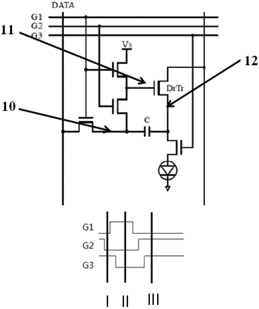
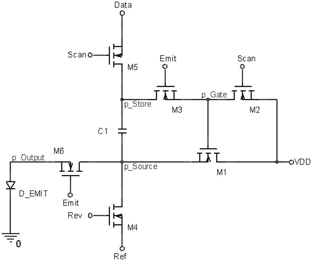
[0027] Embodiments of the present invention provide a pixel compensation circuit and a display, which are used for compensating the threshold shift of the NMOS driving transistor in the pixel, and for locking the voltage difference between the source and the gate of the NMOS driving transistor in the pixel.

[0028] A pixel compensation circuit provided by an embodiment of the present invention includes: a first switch unit, a second switch unit, a third switch unit, a fourth switch unit, a fifth switch unit, a sixth switch unit, a light emitting device, and a capacitor; A switch unit, a second switch unit, a third switch unit, a fourth switch unit, a fifth switch unit, and a sixth switch unit all include three connection terminals, wherein,

[0029] The first connection end of the first switch unit is connected between the second switch unit and the third switch unit, the second connection end is connected between the capacitor and the fourth switch unit, and the third connect...


PUM


Abstract

The invention discloses a pixel compensating circuit and a displayer. The pixel compensating circuit is used for compensating for threshold drift of an NMOS driving tube in pixels. The pixel compensating circuit comprises a first switch unit, a second switch unit, a third switch unit, a fourth switch unit, a fifth switch unit, a sixth switch unit, a luminescent device and a capacitor, wherein the first switch unit, the second switch unit, the third switch unit, the fourth switch unit, the fifth switch unit and the sixth switch unit respectively comprise three connecting ends. The pixel compensating circuit is low in technological requirement, the design of a panel can be greatly simplified through a quite small number of input signals, the number of pixels per inch of the displayer is increased, current related to screen entrance signals can be accurately output, and therefore the uniformity of the actual display frame color can be improved, and it is guaranteed that no display abnormality occurs.

Description

technical field [0001] The present invention relates to the technical field of light-emitting diode (Light Emitting Diode, LED) light-emitting display and driving, in particular to a pixel compensation circuit driving method and a display device. Background technique [0002] An existing pixel compensation circuit uses an N-type metal oxide semiconductor transistor (Negative channel-Metal-Oxide-Semiconductor, NMOS transistor) as a switching device. Such as figure 1 As shown, in the data writing and compensation phase (phase II), the first scanning signal (Gate1, G1) is turned on, and the data signal (DATA) is input, so that the voltages at both ends of the storage capacitor C are V_Data (signal input pole 10 voltage ) and V0-V_th (threshold voltage of the source 12 of the drive tube DrTr). In the light-emitting phase (phase III), after G1 is turned off and the second scanning signal (Gate2, G2) is turned on, the voltage of the gate 11 and source 12 of the drive tube DrTr i...

Claims


Application Information

Patent Timeline
Patent Type & Authority Patents(China)
IPC IPC(8): G09G3/32G09G3/3208
Inventor 翟应腾吴勇
Owner GUANGDONG JUHUA PRINTING DISPLAY TECH CO LTD
Why Eureka
Try Eureka