Shifting register, gate driving circuit, array substrate, display panel and device

A shift register, gate technology, applied in static memory, digital memory information, instruments, etc., can solve the problems affecting the display quality of display devices, poor display effect of display devices, etc., to improve display quality, prevent waveform distortion, reduce cost effect

Active Publication Date: 2014-07-16
XIAMEN TIANMA MICRO ELECTRONICS +1
View PDF4 Cites 9 Cited by
  • Summary
  • Abstract
  • Description
  • Claims
  • Application Information

AI Technical Summary

Problems solved by technology

[0002] Recently, display technology has developed rapidly, and display devices have become more and more popular. However, in actual use, it is found that the TFT (Thin Film Transistor, Thin Film Transistor) in the TFT array substrate of the display device has a leakage current problem, which leads to the display effect of the display device. Defective, affecting the display quality of the display device

Method used


Image

  • Shifting register, gate driving circuit, array substrate, display panel and device
  • Shifting register, gate driving circuit, array substrate, display panel and device
  • Shifting register, gate driving circuit, array substrate, display panel and device

Examples


Embodiment 1

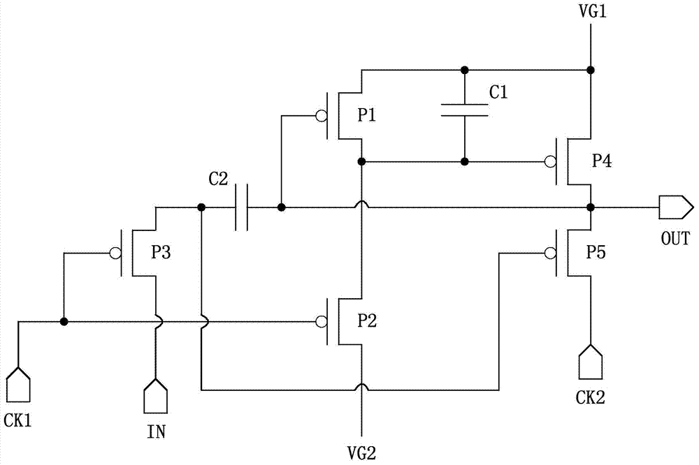
[0032] Embodiment 1 of the present invention provides a shift register. Figure 4 It is a schematic diagram of the internal structure of a shift register according to Embodiment 1 of the present invention. Such as Figure 4 As shown, the shift register includes: a first transistor M1, a second transistor M2, a third transistor M3, a fourth transistor M4, a fifth transistor M5, a voltage dividing element (not shown), a first capacitor C1 and a second capacitor C2, wherein the gate of the fifth transistor M5 is electrically connected to the drain of the third transistor M3 through a voltage dividing element; further, the voltage dividing element is the sixth transistor M6;

[0033] Specifically, the gate of the first transistor M1 is electrically connected to the output terminal OUT, the drain is electrically connected to the first level signal line VG1, and the source is respectively electrically connected to the drain of the second transistor M2 and the gate of the fourth tra...

Embodiment 2

[0053] Embodiment 2 of the present invention provides a gate driving circuit, the gate driving circuit includes n stages of shift registers connected in series, and n is a positive integer. Wherein the shift register adopts the shift register described in the first embodiment above.

[0054] Figure 7 It is a structural block diagram of a gate driving circuit according to Embodiment 2 of the present invention. see Figure 7, the gate drive circuit includes n stages of shift registers (SR1-SRn) connected in series, where n is a positive integer; specifically, the input terminal IN1 of the shift register SR1 of the first stage receives the start signal, and the tenth stage The input terminal IN10 of the shift register SR10 is electrically connected to the output terminal OUT9 of the ninth-stage shift register SR9. It should be noted that the input terminal IN10 of the tenth-stage shift register SR10 in this embodiment is electrically connected to the ninth-stage shift register...

Embodiment 3

[0058] Embodiment 3 of the present invention provides a TFT array substrate, and the TFT array substrate includes a gate driving circuit. Wherein, the gate driving circuit adopts the gate driving circuit described in the second embodiment above. It should be noted that the TFTs in the TFT array substrate are not limited to A-Si (amorphous silicon) type, LTPS (Low Temperature Poly-silicon, low temperature polysilicon) type or oxide type. Preferably, the TFTs in the TFT array substrate can be With the LTPS type, due to the material characteristics of LTPS, its electronic conductivity is higher, which can further improve the performance of the TFT array substrate, thereby improving the display effect.

[0059] The above-mentioned gate driving circuit can realize unilateral driving and double-sided driving for the scanning lines on the TFT array substrate. Figure 8a It is a schematic structural diagram of a TFT array substrate driven on one side according to Embodiment 3 of the ...


PUM


Abstract

The invention discloses a shifting register which comprises a first transistor, a second transistor, a third transistor, a fourth transistor, a fifth transistor and a voltage division component, wherein a grid of the fifth transistor is electrically connected with a drain of the third transistor through the voltage division component. The embodiment of the invention at least achieves one of the following effects: the shifting register can be adopted to prevent output signal's wave form distortion caused by leak current so as to raise display quality of a display device, minimize the number of photomasks and reduce the influence of process capability on yield, and then capacity is raised and cost is decreased.

Description

technical field [0001] The present invention relates to the field of display technology, in particular to a shift register, a gate drive circuit, a TFT array substrate, a display panel and a display device. Background technique [0002] Recently, display technology has developed rapidly, and display devices have become more and more popular. However, in actual use, it is found that the TFT (Thin Film Transistor, Thin Film Transistor) in the TFT array substrate of the display device has a leakage current problem, which leads to the display effect of the display device. Defective, affecting the display quality of the display device. Contents of the invention [0003] In view of this, an embodiment of the present invention provides a shift register, a gate driving circuit, a TFT array substrate, a display panel, and a display device. [0004] In a first aspect, an embodiment of the present invention provides a shift register, including: a first transistor, a second transisto...

Claims


Application Information

Patent Timeline
IPC IPC(8): G11C19/28G09G3/36G09G3/32G09G3/34G09G3/3208
Inventor 周莉草彅英则夏军
Owner XIAMEN TIANMA MICRO ELECTRONICS
Why Eureka
Try Eureka