Semiconductor package with passive devices and stacking method thereof

A passive device and semiconductor technology, applied in the fields of semiconductor device, semiconductor/solid-state device manufacturing, semiconductor/solid-state device components, etc., which can solve problems such as large size, long distance between controller and storage device, and unfavorable signal quality.

Active Publication Date: 2016-09-07
SAMSUNG SEMICON CHINA RES & DEV +1
View PDF3 Cites 0 Cited by
  • Summary
  • Abstract
  • Description
  • Claims
  • Application Information

AI Technical Summary

Problems solved by technology

[0008] To sum up, the size of semiconductor packages with passive devices in the prior art is large, and the distance between the controller and the storage device is relatively long, and the distance between the passive devices and VCC and VSS is relatively long, which is not conducive to improving signal quality

Method used


Image

  • Semiconductor package with passive devices and stacking method thereof
  • Semiconductor package with passive devices and stacking method thereof
  • Semiconductor package with passive devices and stacking method thereof

Examples


Embodiment 1

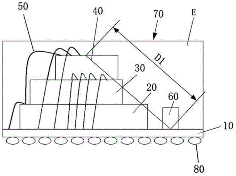
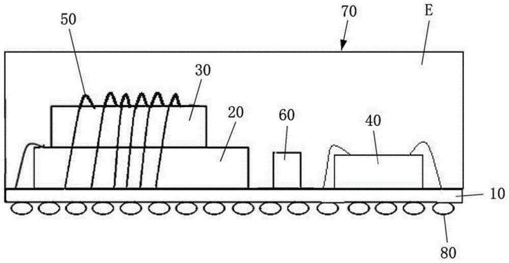
[0025] image 3 is a stacked structure of semiconductor packages 170 according to an exemplary embodiment of the present invention. The following will refer to image 3 Exemplary embodiments of the present invention will be described.

[0026] refer to image 3 , the semiconductor package 170 of the exemplary embodiment of the present invention includes: a substrate 110; a first chip 120 disposed on the substrate 110, and the upper surface of the first chip 120 is electrically connected to the substrate 110 by using a bonding wire 150; Chip 130, arranged on the first chip 120, using the bonding wire 150 to electrically connect the upper surface of the second chip 130 to the substrate 110; controller 140, the controller 140 and the first chip 120 are alternately arranged on the first chip 120 On, one end of the controller 140 is electrically connected to the substrate 110 through the connecting post 191 and the bump 192, and the other end is connected to the first chip 120 t...

Embodiment 2

[0040] Next, a method of stacking semiconductor packages with passive devices according to an exemplary embodiment of the present invention will be described with reference to Embodiment 2. Referring to FIG.

[0041] First, the substrate 110 is prepared.

[0042] Next, the first chip 120 is placed on the substrate 110 by using solder balls or conductive adhesive, wherein the first chip 120 occupies a part of the substrate 110, and the upper surface of the first chip 120 is electrically connected to the substrate 110 by bonding wires 150. Substrate 11. Subsequently, the second chip 130 is disposed on the first chip 120 in the same manner, and the upper surface of the second chip 130 is electrically connected to the substrate 110 by the bonding wire 150 .

[0043] The controller 140 is arranged above the part of the substrate 110 where the first chip 120 is not arranged, so that the controller 140 and the first chip 120 are alternately arranged above the first chip 120, and one...


PUM


Abstract

The invention provides a semiconductor package with passive devices and a stacking method of the semiconductor package. The semiconductor package with the passive devices comprises a first device, a second device and at least one independent passive device, wherein one part of the first device is connected to a substrate, the other part of the first device is connected to the second device, and the independent passive devices are arranged below the first device. The semiconductor package with the passive devices can have a compact packaging structure, obtain better signals and provide the improved electrical characteristics.

Description

technical field [0001] The present invention relates to a semiconductor package and a stacking method thereof, and more particularly, to a semiconductor package with an improved stacking structure capable of reducing the volume of the package while providing better electrical connection performance to achieve better signals pieces. Background technique [0002] For mobile devices, the controller, dynamic random access memory (DRAM), flash memory, and passive discrete components (also known as passives) are stacked in one package. [0003] Typically, the controller is the smallest component and is placed on top of the package. The passive discrete components should be in contact with the PCB so that the passive discrete components are placed outside the stacked package. For signals, however, the best solution is for the controller to be as close as possible to the flash device, and the passives should be as close as possible to VCC and VSS. [0004] figure 1 is an example...

Claims


Application Information

Patent Timeline
Patent Type & Authority Patents(China)
IPC IPC(8): H01L23/488H01L25/00H01L21/60
CPCH01L2224/48091H01L2224/48227H01L2924/15311
Inventor 顾立群杜茂华
Owner SAMSUNG SEMICON CHINA RES & DEV
Why Eureka
Try Eureka