Printed circuit board (PCB) combination pad

A technology of printed circuit boards and pads, applied in the direction of printed circuit components, electrical connection printed components, etc., to achieve the effect of improving efficiency and PCB wiring quality

Inactive Publication Date: 2014-07-16
ZTE CORP
View PDF4 Cites 6 Cited by
  • Summary
  • Abstract
  • Description
  • Claims
  • Application Information

AI Technical Summary

Problems solved by technology

[0006] The purpose of the present invention is to provide a PCB combination pad to overcome the defect that the existing packaging method only has the installation function of the device

Method used


Image

  • Printed circuit board (PCB) combination pad
  • Printed circuit board (PCB) combination pad
  • Printed circuit board (PCB) combination pad

Examples


Embodiment Construction

[0034] Embodiments of the present invention will be described in detail below in conjunction with the accompanying drawings. It should be noted that, in the case of no conflict, the embodiments in the present application and the features in the embodiments can be combined arbitrarily with each other.

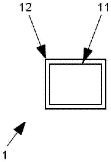
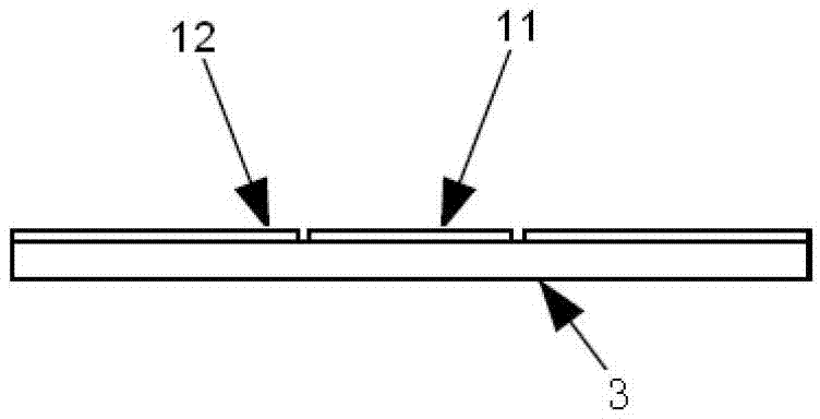
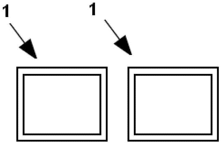
[0035] As shown in Fig. 3 (a), in the PCB combination pad 6 in the present embodiment, except comprising traditional PCB pad 61, also comprise the electrical connection part (such as copper wire (trace) or copper skin) that realizes electric connection (shape)) 64 and vias (via) 65. 61, 64, 65 form a conductive whole, as shown in the three-dimensional view in FIG. 3(b). This combo pad can correspond to a pin on the device schematic symbol.

[0036] EDA (Electronic Design Automation, Electronic Design Automation) software only allows one pin in the device schematic library symbol to correspond to one pad or a combined pad. Therefore, the pad 61 and the via 65 can be associated ...


PUM


Abstract

The invention discloses a printed circuit board (PCB) combination pad. A first kind of PCB combination pad comprises a pad and further comprises an electric connection part and a through hole. The electric connection part is respectively connected with the pad and the through hole, and the electric connection part, the pad and the through hole constitute a conductive integral body. A second kind of PCB combination pad comprises a PCB substrate. The PCB substrate is provided with a through hole. In a packaging design, another pad and the PCB pad are connected by use of an electric connection part to form a conductive integral body. A third kind of PCB combination pad comprises a pad and further comprises an electric connection part. The idle end of the electric connection part is taken as the position indication of a through hole during wiring to unify a wiring mode. By using the PCB combination pad provided by the invention, the functions of partial wiring connection or complete wiring connection can be finished on the pad, the defect of wiring quality control difficulty caused by the randomness of a lead wire and the through hole during manual wiring is avoided, and the PCB design efficiency and PCB wiring quality are improved.

Description

technical field [0001] The present invention relates to the field of electronic equipment, in particular to a printed circuit board (Printed Circuit Board, referred to as PCB for short) composite pad (Pad). Background technique [0002] The traditional device PCB (Printed Circuit Board, printed circuit board) package (Footprint) is an array of pads according to the size recommended by the device manufacturer, so as to realize the reliable combination of the device and the PCB board when the device is soldered on the PCB. [0003] The main element that makes up the package is the pad. Pads are usually regular in shape, and the most common pad shapes are square, rectangular, or circular. As shown in FIG. 1( a ), 1 is a soldering pad of a PCB package, including: a soldering pad 11 and a soldermask opening 12 . Among them, the material of the pad 11 is base copper plus electroplated copper during PCB processing, and then covered with a surface treatment coating; the area outsi...

Claims


Application Information

Patent Timeline
Patent Type & Authority Applications(China)
IPC IPC(8): H05K1/11
Inventor 眭诗菊高云航
Owner ZTE CORP
Why Eureka
Try Eureka