

Touch film structure
A thin-film structure and touch technology, which is applied in instruments, electrical digital data processing, input/output process of data processing, etc., can solve the problem of poor electrical properties of sensing elements, abnormal touch detection, high moisture and oxygen penetration Ratio and other issues, to improve the effect of poor flexural characteristics and reduce stack thickness
- Summary
- Abstract
- Description
- Claims
- Application Information
AI Technical Summary
Problems solved by technology
Method used
Image

Examples
no. 1 example
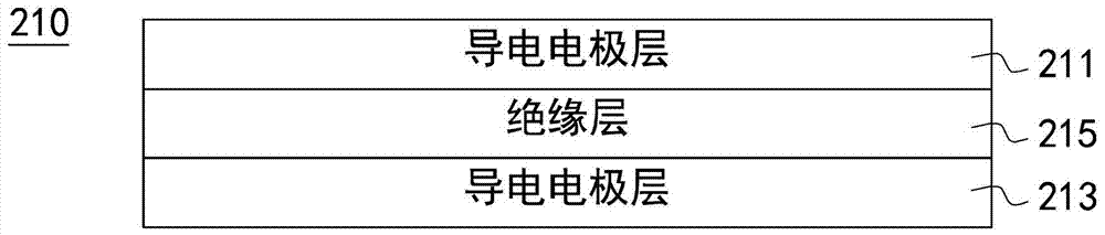
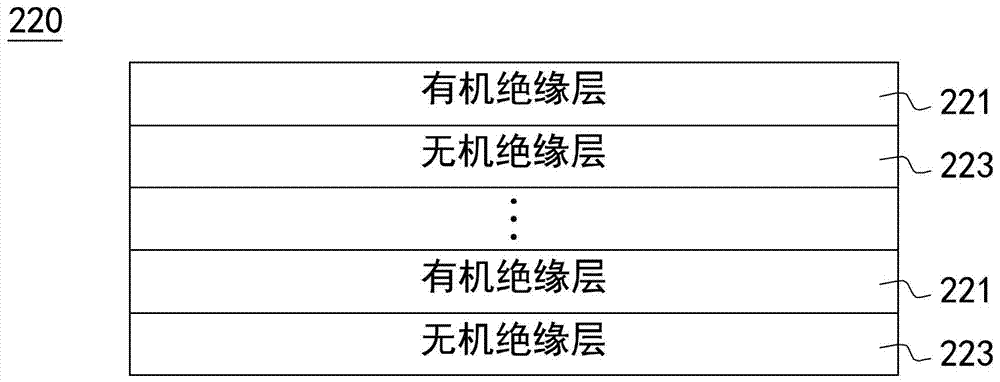
[0070] Please refer to Figure 4A ~ Figure 4D , which respectively show combined schematic diagrams of the touch film structure 101 having the function of blocking water and oxygen. exist Figure 4A In this example, the barrier layer 220 is formed on the first surface 212 of the touch element layer 210 , and the touch element layer 210 is located between the barrier layer 220 and the flexible substrate 250 . In addition, in Figure 4B Among them, the barrier layer 220 is, for example, formed on the second surface 214 of the touch element layer 210 and located between the touch element layer 210 and the flexible substrate 250 .
[0071] exist Figure 4C Among them, the barrier layer 220 is contained in the touch element layer 210, for example, and becomes the touch element layer 210a with a barrier function, that is, in figure 1 The insulating layer 215 of the middle touch element layer 210 is replaced by the barrier layer 220 having the function of blocking water and oxyge...
no. 2 example
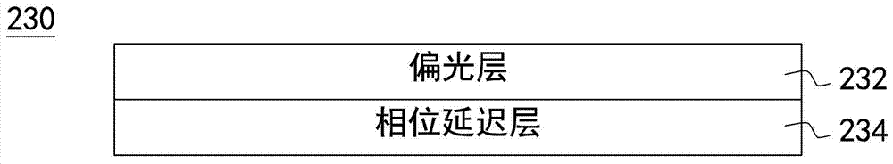
[0074] Please refer to Figure 5A ~ Figure 5F , which respectively show combined schematic diagrams of the touch film structure 102 with the function of blocking water and oxygen and circularly polarizing light. exist Figure 5A Among them, the barrier layer 220 is formed on the first surface 212 of the touch element layer 210, the circular polarizing film layer 230 is formed on the second surface 214 of the touch element layer 210, and the circular polarizing film layer 230 is located on the touch element layer 210 and the flexible substrate 250. In addition, in Figure 5B Among them, the circular polarizing film layer 230 is formed on the first surface 212 of the touch element layer 210, the barrier layer 220 is formed on the circular polarizing film layer 230, and the touch element layer 210 is located between the circular polarizing film layer 230 and the flexible substrate 250. between.
[0075] exist Figure 5C Among them, the circular polarizing film layer 230 is c...
no. 3 example
[0079] Next, please refer to Figure 6A ~ Figure 6F , which respectively show combined schematic diagrams of the touch film structure 103 with the function of blocking water, oxygen and circularly polarized light. exist Figure 6A Among them, the circular polarizing film layer 230 is formed on the first surface 212 of the touch element layer 210, the barrier layer 220 is formed on the second surface 214 of the touch element layer 210, and the barrier layer 220 is located between the touch element layer 210 and the soft Between the substrate 250. In addition, in Figure 6B Among them, the barrier layer 220 is formed on the first surface 212 of the touch element layer 210 , the circular polarizing film layer 230 is formed on the barrier layer 220 , and the touch element layer 210 is located between the barrier layer 220 and the flexible substrate 250 .
[0080] exist Figure 6C Among them, the barrier layer 220 is contained in the touch element layer 210, for example, and be...
PUM
 Abstract
Description
Claims
Application Information