Memory and preparation method thereof

A memory and control gate technology, applied in the direction of semiconductor devices, electrical solid devices, electrical components, etc., can solve the problems of difficult filling of intermediate insulating dielectric layers, low CG-FG coupling capacitance, thick stacking thickness, etc., to achieve filling insulating dielectric Easy layering, improved yield and reliability, and increased effective contact area

Pending Publication Date: 2019-07-16
GIGADEVICE SEMICON SHANGHAI INC +1
View PDF0 Cites 0 Cited by
  • Summary
  • Abstract
  • Description
  • Claims
  • Application Information

AI Technical Summary

Problems solved by technology

[0002] Traditional Flash memories use self-alignment technology to make floating gates (Floating Gate, FG). Although the process is simple and the cost is low, the effective contact area between the floating gate and the control gate (Control Grid, CG) is low, resulting in CG-FG coupling The capacitance is low, which leads to the control gate requiring a higher operating voltage to erase and write the floating gate, resulting in high power consumption of the storage device. In addition, the stacking thickness of the traditional floating gate and control gate is thicker in the vertical direction. It leads to difficulty in filling the subsequent intermediate insulating dielectric layer, resulting in problems of low yield and poor reliability

Method used


Image

  • Memory and preparation method thereof
  • Memory and preparation method thereof
  • Memory and preparation method thereof

Examples


Embodiment Construction

[0044] The present invention will be further described in detail below in conjunction with the accompanying drawings and embodiments. It should be understood that the specific embodiments described here are only used to explain the present invention, but not to limit the present invention. In addition, it should be noted that, for the convenience of description, only some structures related to the present invention are shown in the drawings but not all structures.

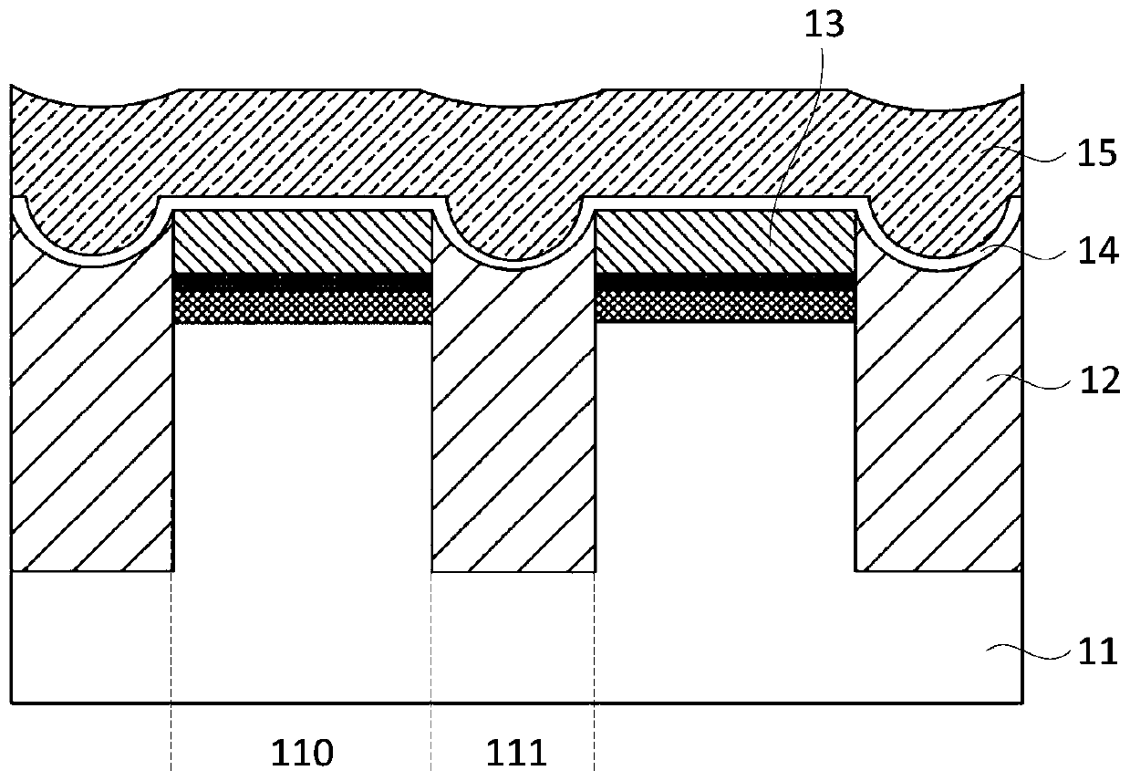
[0045] figure 1 It is a structural schematic diagram of an existing memory. see figure 1 , the memory includes: a base substrate 11, the base substrate 11 includes a plurality of active regions 110 and a plurality of shallow trench isolation regions 111, and the active regions 110 and the shallow trench isolation regions 111 are arranged at intervals. The memory also includes an isolation layer 12 filling the shallow trench isolation region 111, a floating gate 13 on the active region 110, a dielectric layer 14 ...


PUM


Abstract

The invention discloses a memory and a preparation method thereof. The memory comprises a substrate, an isolation layer, a groove structure, floating gates, a dielectric layer, and a control gate, wherein the substrate comprises a plurality of active regions and a plurality of shallow trench isolation regions, and the active regions and the shallow trench isolation regions are arranged at intervals; the isolation layer is filled in the shallow trench isolation regions, wherein the isolation layer extends to a part of the upper surfaces, close to one side of the shallow trench isolation regions, of the active regions; the groove structure is located in the active regions, and the groove structure partially penetrates through the substrate corresponding to the active regions; the floating gates are located on the surface of the inner wall of the groove structure and extend to the upper surface of the isolation layer along the inner wall of the groove structure, and the floating gates corresponding to the adjacent active regions are disconnected; the dielectric layer is located on the upper surfaces of the floating gates and the upper surface of the isolation layer; and the control gate located on the dielectric layer. The memory provided by the embodiment of the invention has relatively low power consumption and relatively high yield and reliability.

Description

technical field [0001] Embodiments of the present invention relate to the technical field of semiconductor manufacturing, and in particular, to a memory and a manufacturing method thereof. Background technique [0002] Traditional Flash memories use self-alignment technology to make floating gates (Floating Gate, FG). Although the process is simple and the cost is low, the effective contact area between the floating gate and the control gate (Control Grid, CG) is low, resulting in CG-FG coupling The capacitance is low, which leads to the control gate requiring a higher operating voltage to erase and write the floating gate, resulting in high power consumption of the storage device. In addition, the stacking thickness of the traditional floating gate and control gate is thicker in the vertical direction. As a result, it is difficult to fill the subsequent intermediate insulating dielectric layer, resulting in problems of low yield and poor reliability. Contents of the inven...

Claims


Application Information

Patent Timeline
Patent Type & Authority Applications(China)
IPC IPC(8): H01L27/11517H01L27/11521
CPCH10B41/00H10B41/30
Inventor 刘钊熊涛许毅胜舒清明
Owner GIGADEVICE SEMICON SHANGHAI INC
Why Eureka
Try Eureka