Three-dimensional integrated circuit multi-physical-domain collaborative design method based on through-silicon via

An integrated circuit and collaborative design technology, which is applied in the direction of electrical digital data processing, calculation, and special data processing applications, can solve the problems of not considering the influence of reliability, costing a lot of money, and increasing the cost of three-dimensional integrated circuit design, so as to reduce Design complexity, reduce design cost, and improve design efficiency

Active Publication Date: 2014-07-23
珠海天成先进半导体科技有限公司
View PDF3 Cites 10 Cited by
  • Summary
  • Abstract
  • Description
  • Claims
  • Application Information

AI Technical Summary

Problems solved by technology

Since the developed design software is very different and has a certain degree of pertinence, the design process established with it is not the same and does not have universality.
Moreover, the development of dedicated three-dimensional circuit design software will cost a lot of money, which will dramatically increase the cost of three-dimensional integrated circuit design
[0005] Second, the three-dimensional integrated circuit design process based on planar integrated circuit design methodology cannot complete the collaborative design of electrical, mechanical and thermal multi-physics domains
But the disadvantage is that due to the design of planar integrated circuits, the overall design process does not introduce thermal and force design, and does not consider the influence of coupling between thermal, force, and electrical multi-physics domains on the reliability of three-dimensional integrated circuits, and lacks multi-physics field coordination. design, so the three-dimensional integrated circuit designed through this process may not meet the design requirements in terms of thermal and mechanical reliability

Method used


Image

  • Three-dimensional integrated circuit multi-physical-domain collaborative design method based on through-silicon via
  • Three-dimensional integrated circuit multi-physical-domain collaborative design method based on through-silicon via
  • Three-dimensional integrated circuit multi-physical-domain collaborative design method based on through-silicon via

Examples


Embodiment 1

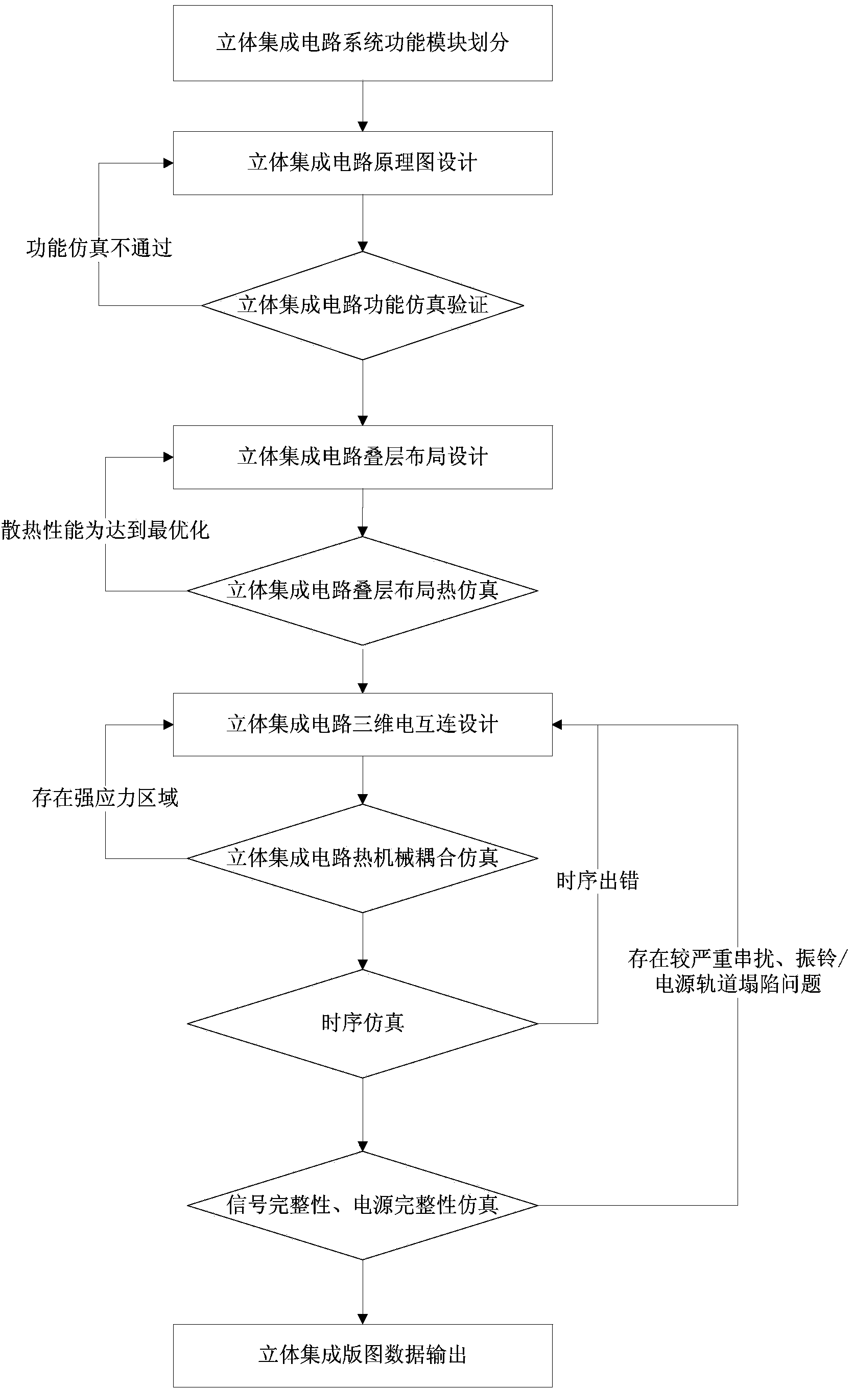
[0082] According to the design method proposed by the present invention, the three-dimensional integrated 4M SRAM memory design design steps are as follows:

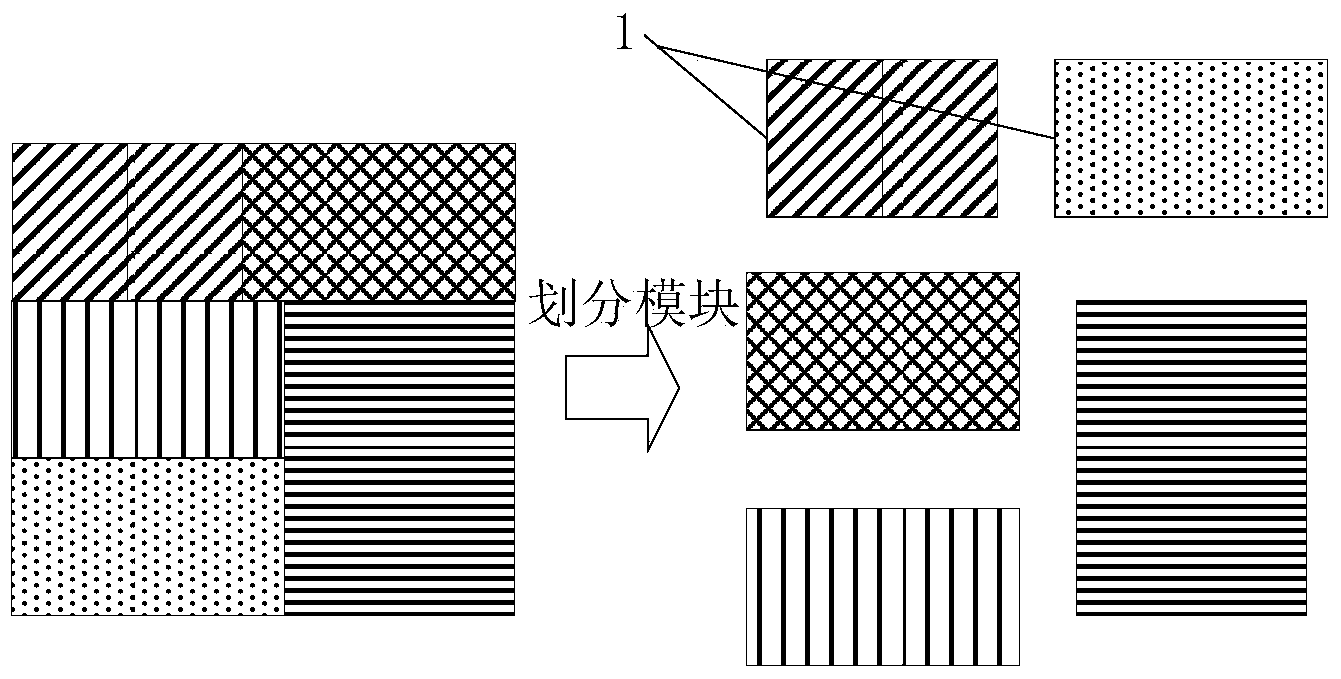
[0083] 1) Functional module division of three-dimensionally integrated 4M SRAM memory system

[0084] The 4M SRAM memory system can be divided into 4 independent 1M SRAM memory sub-modules according to functions, and one 1M SRAM memory is arranged on a 1-layer chip layer, with a total of 4 layers.

[0085] 2) Schematic design of three-dimensional integrated 4M SRAM memory

[0086] Using Altium Designer software, draw a two-dimensional circuit schematic diagram of four 1M SRAM memories. At this time, the TSV delay characteristic is not introduced into the interconnection relationship of each 1M SRAM in the schematic diagram.

[0087] Three-dimensional integrated 4M SRAM memory function simulation verification: Input the above schematic RTL code into ModelSim or Incisive software, and verify whether all functions are corr...

Embodiment 2

[0104] According to the design method proposed by the present invention, the design steps of a three-dimensional integrated electronic system are as follows:

[0105] 1) Division of functional modules of three-dimensional integrated electronic system

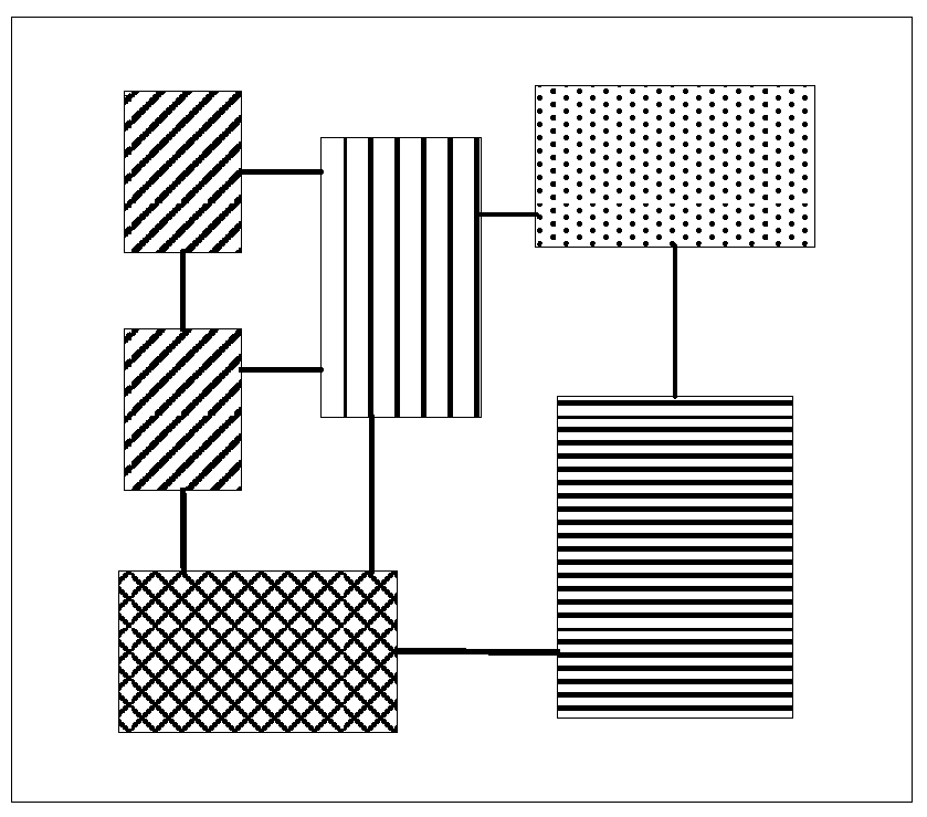
[0106] The three-dimensional integrated electronic system can be divided into SoC modules, various peripheral memory modules and bus modules according to functions. Specifically, there are 5 sub-modules of SoC, CAN bus, SRAM, FLASH, and FPGA.

[0107] 2) Schematic design of three-dimensional integrated electronic system

[0108] Using Altium Designer software, draw a two-dimensional circuit schematic diagram of the electronic system composed of the above five sub-modules. At this time, the interconnection relationship between the five sub-modules in the schematic diagram does not introduce the through-silicon via delay characteristic.

[0109] Input the above schematic RTL code into ModelSim or Incisive software to verify that...


PUM


Abstract

The invention discloses a three-dimensional integrated circuit multi-physical-domain collaborative design method based on the through-silicon via. Influences, caused by coupling among the thermology physical domain, the mechanics physical domain and the electricity physical domain, on reliability of a three-dimensional integrated circuit are taken into consideration, the thermology design step and the mechanics design step are added, and the thermology, mechanics and electricity multi-physical-domain collaborative design method is built. According to the multi-physical-domain collaborative design method, mutual iteration is carried out among the thermology design step, the mechanics design step and the electricity design step till the thermology design step, the mechanics design step and the electricity design step all meet the design requirements, and the design requirement of the three-dimensional integrated circuit for high reliability is ensured. The defect that an existing three-dimensional integrated circuit design process is lacking in the thermology design step and the mechanics design step is overcome.

Description

technical field [0001] The invention belongs to the technical field of three-dimensional integrated circuits, and relates to a multi-physical domain collaborative design method of three-dimensional integrated circuits based on through-silicon vias. Background technique [0002] The three-dimensional integration technology based on Through-Silicon Via (TSV) enables vertical transmission of information between stacked chips through through-silicon vias, which can greatly shorten the length of the global interconnection of the chips and ease the blockage of wiring channels. One of the most effective ways to develop. Although three-dimensional integration technology has great advantages, the introduction of vertical interconnection in electronic systems increases the design complexity of three-dimensional integrated circuits. the biggest obstacle to development. [0003] At present, there are two main problems faced by the three-dimensional integrated circuit design technology...

Claims


Application Information

Patent Timeline
Patent Type & Authority Applications(China)
IPC IPC(8): G06F17/50
Inventor 单光宝刘松谢成民孙有民
Owner 珠海天成先进半导体科技有限公司
Why Eureka
Try Eureka