Metal hard mask structure, manufacturing method and copper interconnection structure manufacturing method

A technology of copper interconnection structure and metal hard mask, which is applied in semiconductor/solid-state device manufacturing, electrical components, circuits, etc., can solve the problems of copper interconnection structure failure, performance degradation, peeling, etc., to reduce filling defects and improve Morphology, the effect of improving product performance

Active Publication Date: 2016-09-07
SHANGHAI HUALI MICROELECTRONICS CORP
View PDF5 Cites 0 Cited by
  • Summary
  • Abstract
  • Description
  • Claims
  • Application Information

AI Technical Summary

Problems solved by technology

However, this relatively straight trench morphology is a great challenge to the direct filling of the subsequent interconnected copper in the trench, which is prone to filling defects such as voids (gap), which in turn causes the filled copper to peel off from the trench ( strip damage), causing the copper interconnect structure to fail or degrade its performance

Method used


Image

  • Metal hard mask structure, manufacturing method and copper interconnection structure manufacturing method
  • Metal hard mask structure, manufacturing method and copper interconnection structure manufacturing method
  • Metal hard mask structure, manufacturing method and copper interconnection structure manufacturing method

Examples


Embodiment Construction

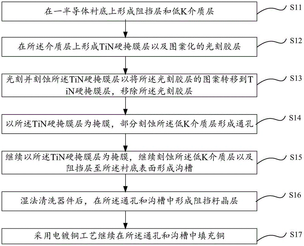
[0042] In order to make the purpose and features of the present invention more obvious and easy to understand, the following will further describe the specific embodiments of the present invention in conjunction with the accompanying drawings. However, the present invention can be realized in different forms, and should not be considered as being limited to the described embodiments .

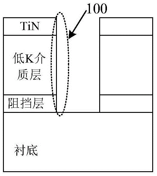
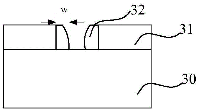
[0043] Please refer to image 3 , the present invention proposes a metal hard mask structure, including: a patterned metal hard mask layer 31 located on a substrate 30 and inner wall metal hard mask layers formed on both inner sidewalls of the patterned metal hard mask layer 31 A mask layer 32 (spacer), the etching selectivity ratio of the inner wall metal hard mask layer 32 and the patterned metal hard mask layer 31 is different.

[0044] Wherein, the patterned metal mask layer 31 can be titanium nitride TiN (MHM), utilizing the high etching property between TiN and the low-K dielectric layer...


PUM

PropertyMeasurementUnit
heightaaaaaaaaaa
widthaaaaaaaaaa

Abstract

The invention provides a metal hard mask structure, a manufacturing method and a copper interconnecting structure manufacturing method. By forming inner wall metal mask layers different in etching selection ratio on the basis of an inner side wall of an existing metal hard mask layer, the shape of the etching forming structure is improved by utilizing the difference of the etching selection ratio of two metal hard mask layers on layer structures below the metal hard mask layers respectively in a follow-up etching process, the key dimension of a top end opening of the etching forming structure is increased, a larger process window is provided for a follow-up filling process, filling defects are effectively reduced, and the product performance is improved.

Description

technical field [0001] The invention relates to the field of semiconductor manufacturing, in particular to a metal hard mask structure, a manufacturing method and a copper interconnection structure manufacturing method. Background technique [0002] As the critical dimensions of semiconductor devices continue to shrink, void-free filling of copper interconnects becomes increasingly difficult. It is difficult to meet the requirements simply by relying on barrier&seed and electroplating copper (ECP) process progress, which requires other processes to provide a larger process window for barrier&seed and ECP. [0003] In order to reduce the RC delay (delay) of copper interconnection, porous low-k dielectric material is introduced, but the ensuing peeling damage (strip damage) becomes non-negligible. In order to overcome a series of challenges caused by the introduction of porous low dielectric materials, the process integration adopts a titanium nitride (TiN) metal hard mask (m...

Claims


Application Information

Patent Timeline
Patent Type & Authority Patents(China)
IPC IPC(8): H01L21/768
CPCH01L21/76811
Inventor 鲍宇
Owner SHANGHAI HUALI MICROELECTRONICS CORP
Why Eureka
Try Eureka