Variable clock DDS arbitrary waveform signal source output frequency control method and realization device
An arbitrary waveform and signal source technology, applied in the field of DDS signal source, can solve complex problems
- Summary
- Abstract
- Description
- Claims
- Application Information
AI Technical Summary
Problems solved by technology
Method used
Image
Examples
Embodiment Construction
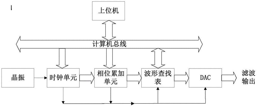
[0050] The following will be attached Figure 5 An embodiment of the present invention will be described in detail.
[0051] This embodiment includes an upper computer, a crystal oscillator, a clock unit, a phase accumulation unit, a waveform look-up table and a DAC. The upper computer is connected to the PCI local bus through PLX9054, and the clock unit and phase accumulation unit are implemented based on FPGA (Field-Programmable Gate Array). The crystal oscillator uses a 100MHz crystal oscillator to provide a 100MHz clock for the clock unit. The waveform look-up table is realized by a 1M×16B dual-port RAM to store waveform data information. The dual-port RAM has two sets of data lines and address lines. One end realizes that the upper computer writes waveform data to the RAM through the PCI local bus, and the other end Output waveform data to the DAC.
[0052] The upper computer is connected with the clock unit, the phase accumulating unit and the dual-port RAM through the PCI...
PUM
 Abstract
Description
Claims
Application Information
 - R&D
- Intellectual Property
- Life Sciences
- Materials
- Tech Scout
- Unparalleled Data Quality
- Higher Quality Content
- 60% Fewer Hallucinations
Browse by: Latest US Patents, China's latest patents, Technical Efficacy Thesaurus, Application Domain, Technology Topic, Popular Technical Reports.
© 2025 PatSnap. All rights reserved.Legal|Privacy policy|Modern Slavery Act Transparency Statement|Sitemap|About US| Contact US: help@patsnap.com


