Stacked light emitting diode array structure
A technology of light-emitting diodes and array structures, applied in semiconductor devices, electrical components, circuits, etc., can solve the problems of increasing cost and setting volume
- Summary
- Abstract
- Description
- Claims
- Application Information
AI Technical Summary
Problems solved by technology
Method used
Image
Examples
Embodiment Construction
[0040] Below in conjunction with accompanying drawing, structural principle and working principle of the present invention are specifically described:
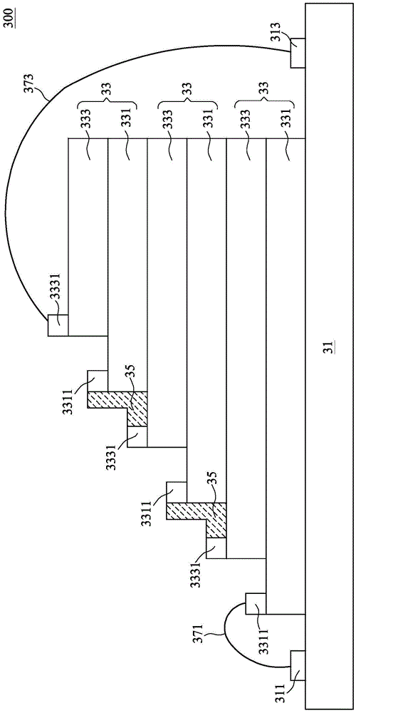
[0041] see image 3 , is a structural schematic view of a preferred embodiment of the stacked LED array structure of the present invention. As shown in the figure, the LED array 300 includes a substrate 31 and a plurality of LED dies 33 .
[0042] Each LED die 33 is sequentially stacked on the substrate 31 , and each includes a first semiconductor layer 331 and a second semiconductor layer 333 . The first semiconductor layer 331 is an N-type semiconductor layer, and the second semiconductor layer 333 is a P-type semiconductor layer.
[0043]The deposition process is used to deposit the second semiconductor layer 333 of each light emitting diode die 33 on a part of the surface of the first semiconductor layer 331, and to deposit the first semiconductor layer 331 of each light emitting diode die 33 on top of each other. It is...
PUM
 Abstract
Description
Claims
Application Information
 - R&D
- Intellectual Property
- Life Sciences
- Materials
- Tech Scout
- Unparalleled Data Quality
- Higher Quality Content
- 60% Fewer Hallucinations
Browse by: Latest US Patents, China's latest patents, Technical Efficacy Thesaurus, Application Domain, Technology Topic, Popular Technical Reports.
© 2025 PatSnap. All rights reserved.Legal|Privacy policy|Modern Slavery Act Transparency Statement|Sitemap|About US| Contact US: help@patsnap.com


