Low-cost tunable DFB semiconductor laser device of integrated modulator and manufacturing method

A technology for tuning lasers and modulators, applied in the field of optoelectronics, can solve problems such as the inability to achieve very high direct modulation rates, weaken the advantages of tunable solutions, and achieve the effect of simplifying packaging structure design, easy packaging, and reducing complexity and cost.

Active Publication Date: 2014-07-30
南京华飞光电科技有限公司
View PDF3 Cites 33 Cited by
  • Summary
  • Abstract
  • Description
  • Claims
  • Application Information

AI Technical Summary

Problems solved by technology

Moreover, direct modulation of lasers generally cannot achieve a very high direct modulation rate, and the direct modulation rate of 10Gb/s must be well optimized, and the packaging of multi-port

Method used


Image

  • Low-cost tunable DFB semiconductor laser device of integrated modulator and manufacturing method
  • Low-cost tunable DFB semiconductor laser device of integrated modulator and manufacturing method
  • Low-cost tunable DFB semiconductor laser device of integrated modulator and manufacturing method

Examples


Embodiment 1

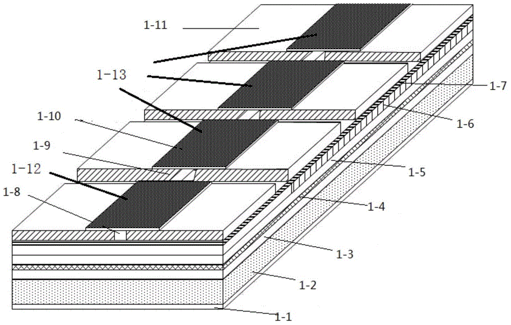
[0034] [Example 1] The working wavelength is 1555 ~ 1561nm based on the same epitaxial structure integrated SOA modulator four-section series tunable DFB semiconductor laser (such as figure 1 shown):

[0035]First, design and manufacture the photolithography plate according to the process steps. The process flow of manufacturing DFB semiconductor lasers based on the reconstruction-equivalent chirp technology is one step more than the standard process flow. The second exposure process of the seed grating, the second Exposure is achieved by sampling a raster plate. The equivalent pi phase shift is introduced by adding a mutation of half the sampling period in the middle of the uniform sampling grating, so as to produce a DFB semiconductor laser with an equivalent pi phase shift. The different lasing wavelengths of the laser are realized by changing the sampling period. The design makes three lasers The lasing wavelengths are 1555nm, 1558nm and 1561nm respectively (the specific ...

Embodiment 2

[0042] [Example 2] The four-section series-connected tunable DFB semiconductor laser (such as figure 2 shown, produced by SAG technology):

[0043] First, design and manufacture the photolithography plate according to the process steps. The process flow of manufacturing DFB semiconductor lasers based on the reconstruction-equivalent chirp technology is one step more than the standard process flow. The second exposure process of the seed grating, the second Exposure is achieved by sampling a raster plate. The equivalent pi phase shift is introduced by adding a mutation of half the sampling period in the middle of the uniform sampling grating, so as to produce a DFB semiconductor laser with an equivalent pi phase shift. The different lasing wavelengths of the laser are realized by changing the sampling period. The design makes three lasers The lasing wavelengths are 1555nm, 1558nm and 1561nm respectively (the specific arrangement order can be optimized according to the situati...

Embodiment 3

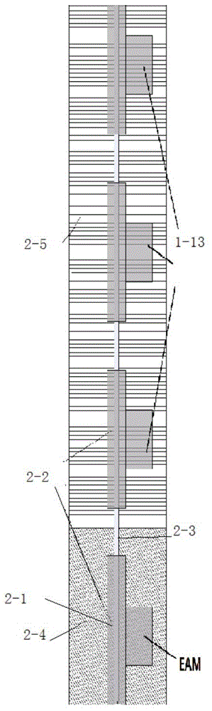
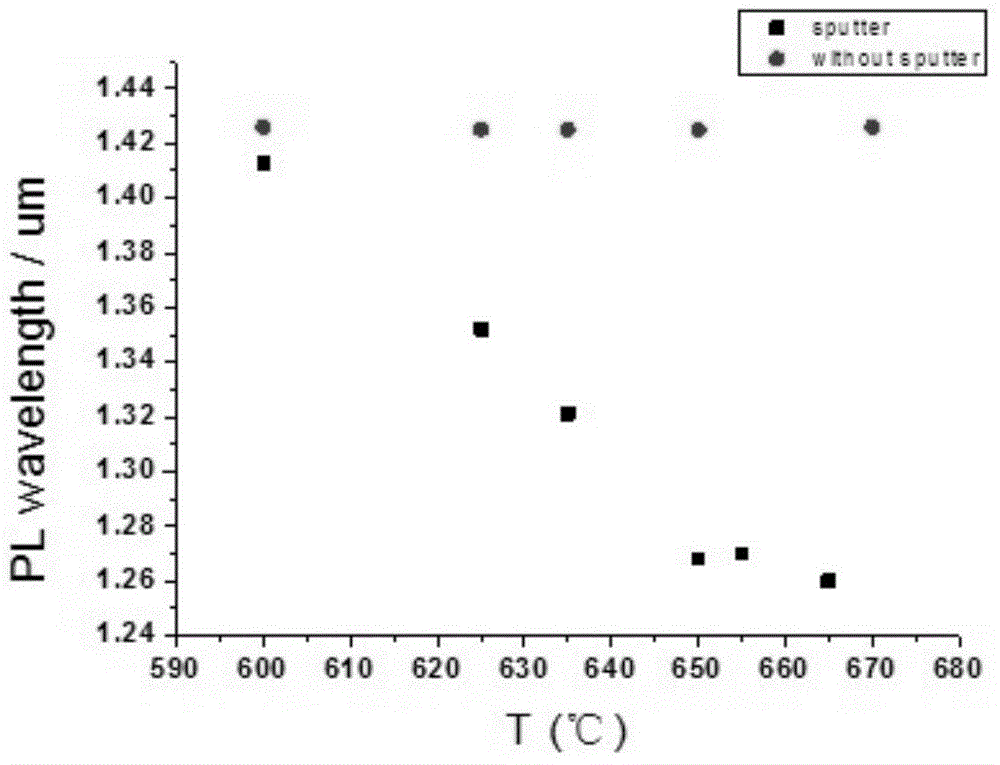
[0050] [Example 3] The tunable DFB semiconductor laser (such as the tunable DFB semiconductor laser with an integrated EAM modulator and coupled through a passive Y-branch waveguide) with an operating wavelength of 1544 to 1559 nm Figure 4 As shown, the blue shift of the PL spectrum is produced by the QWI technique):

[0051] First, design and manufacture the photolithography plate according to the process steps. The process flow of manufacturing DFB semiconductor lasers based on the reconstruction-equivalent chirp technology is one step more than the standard process flow. The second exposure process of the seed grating, the second Exposure is achieved by sampling a raster plate. The equivalent pi phase shift is introduced by adding a mutation of half the sampling period in the middle of the uniform sampling grating, so as to produce a DFB semiconductor laser with an equivalent pi phase shift. The different lasing wavelengths of the laser are realized by changing the samplin...


PUM

PropertyMeasurementUnit
Ridge widthaaaaaaaaaa
Thicknessaaaaaaaaaa

Abstract

The invention discloses a low-cost tunable DFB semiconductor laser device of an integrated modulator. The tunable DFB semiconductor laser device is manufactured with the reconstruction-equivalent chirped technology, multiple DFB semiconductor laser devices share one modulator, and the tunable wavelength range can be expanded by increasing the number of laser devices or adopting the active and passive integration method. The integrated modulator is an semiconductor optical amplifier modulator (SOA), or an electric absorption modulator (EAM), or a Mach-Zehnder modulator (MZM) and can be realized by means of the quantum well intermixing technology (QWI), the Butt-joint growth technology or the selective area growth technology (SAG), and quantum well materials are based on the InP/InGaAsP or InP/AlGaInAs material system. Due to the fact that only one radio frequency port is needed for modulation at least, cost can be reduced by simplifying package design, and practicality and usability are improved greatly.

Description

technical field [0001] The invention belongs to the field of optoelectronic technology, and is related to the distributed feedback semiconductor laser of the integrated modulator, in particular to the design and manufacture of the complex distributed feedback tunable semiconductor laser, more specifically, the integrated modulator based on reconstruction-equivalent chirp A low-cost tunable distributed feedback semiconductor laser method and device for the technology. Background technique [0002] In modern DWDM wavelength division multiplexing systems, wavelength-selectable light sources have always played an important role in optical transmission systems as key components, and tunable lasers can greatly increase the flexibility of network deployment due to their optional wavelength characteristics , and reduce the energy consumption and maintenance cost of the system, therefore, the research and development of tunable lasers has been concerned by research institutes and maj...

Claims


Application Information

Patent Timeline
IPC IPC(8): H01S5/06H01S5/12H01S5/40
CPCH01S5/06258H01S5/0265H01S5/0287H01S5/0612H01S5/1209H01S5/1215H01S5/124H01S5/4031H01S5/4087H01S5/5027
Inventor 唐松李连艳陈向飞
Owner 南京华飞光电科技有限公司
Why Eureka
Try Eureka