A method of speeding up dram sense amplifiers

A sensitive amplifier and voltage technology, applied in the field of memory, can solve problems affecting the reliability of DRAM memory cells

Active Publication Date: 2017-02-08
XI AN UNIIC SEMICON CO LTD
View PDF2 Cites 0 Cited by
  • Summary
  • Abstract
  • Description
  • Claims
  • Application Information

AI Technical Summary

Problems solved by technology

The level of high voltage vblh determines the amplification speed of the sense amplifier, but too high vblh will affect the reliability of DRAM memory cells

Method used


Image

  • A method of speeding up dram sense amplifiers
  • A method of speeding up dram sense amplifiers
  • A method of speeding up dram sense amplifiers

Examples


Embodiment Construction

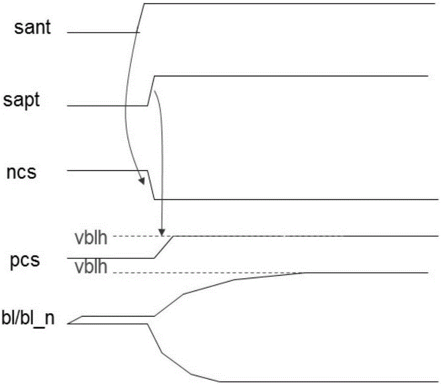
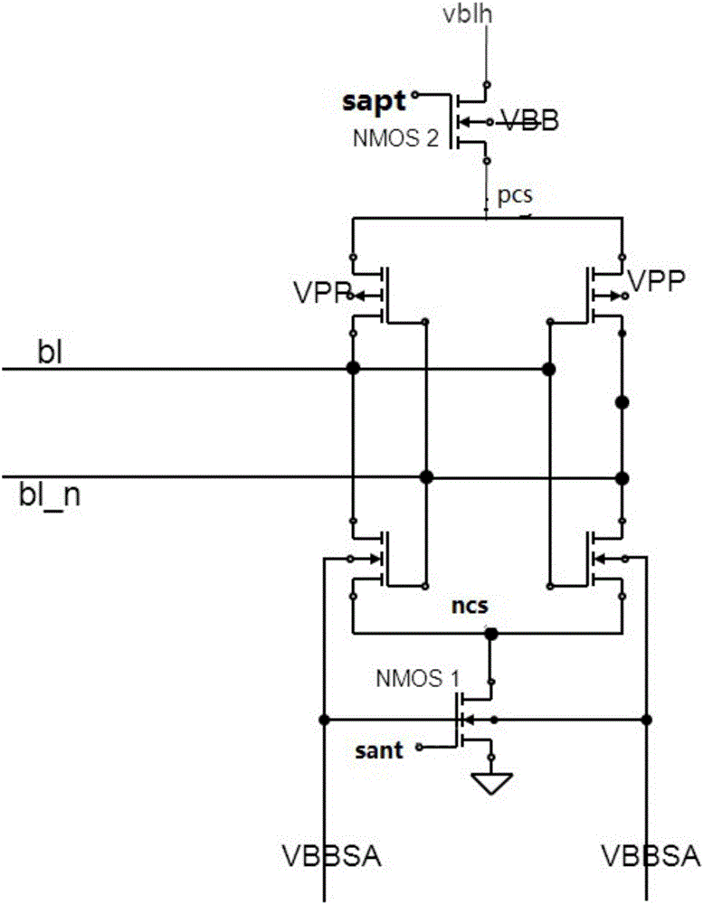
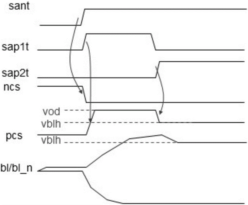
[0025] see image 3 and Figure 4 As shown, in order to improve tRCD (that is, to speed up the amplification speed of the sense amplifier), a method for accelerating the DRAM sense amplifier of the present invention includes the following steps:

[0026] The gate signal sant of NMOS1 is raised to turn on NMOS1, so that the drain signal ncs of NMOS1 is pulled down to the ground voltage, and the reference bit line bl_n starts to be pulled to the ground voltage;

[0027] Then, the gate signal sap1t of NMOS3 is raised to a high level, making NMOS3 turn on, the source signal pcs of NMOS3 is pulled up to vod, the voltage of the bit line bl is quickly pulled up to higher than the voltage vblh, and then the gate signal of NMOS3 sap1t becomes a low level; the gate signal sap2t of NMOS2 becomes a high level, making NMOS2 conductive, the source signal pcs of NMOS2 is pulled to the voltage vblh, and the bit line bl is slowly reduced to the vblh voltage.

[0028] This method improves the...


PUM


Abstract

The invention provides a method for accelerating a DRAM (dynamic random access memory) sensitive amplifier. The method comprises the steps as follows: a grid signal SANT of a first NMOS (N-channel metal oxide semiconductor) transistor rises to turn on the first NMOS transistor, a drain signal NCS of the first NMOS transistor is reduced to the earth voltage, and a reference bit line bl_n starts to be pulled to the earth voltage; then a grid signal SAP1T of a second NMOS transistor rises to break over the second NMOS transistor, a source signal PCS of the second NMOS transistor is raised to a high voltage VOD, a voltage of a bit line bl is quickly raised to be higher than a voltage VBLH, and then the grid signal SAP1T of the second NMOS transistor is changed to be in a low level; then a grid signal SAP2T of a third NMOS transistor rises to break over the third NMOS transistor, a source signal PCS of the third NMOS transistor is pulled to a voltage VBLH, and the bit line bl is slowly reduced to the voltage VBLH. According to the method, the reliability of a DRAM memory cell is guaranteed.

Description

[0001] 【Technical field】 [0002] The present invention relates to the technical field of memory, in particular to a method for accelerating a DRAM sense amplifier. [0003] 【Background technique】 [0004] see figure 1 and figure 2 As shown, in conventional DRAM, the working mechanism of the sense amplifier is as follows: [0005] After the voltage difference between the bit line bl and the reference bit line bl_n reaches a certain value, the signal sant turns on NMOS1, so that the signal ncs is pulled down to the ground voltage, the reference bit line bl_n starts to be pulled to a low voltage, and then the signal sapt turns on NMOS2, so that Signal pcs is pulled high to vblh and bit line bl starts to be pulled high. Finally, the bit line bl is pulled up to the high voltage vblh, and the reference bit line bl_n is pulled down to the ground voltage, thus completing the full swing amplification of the bit line by the sense amplifier. The level of the high voltage vblh determ...

Claims


Application Information

Patent Timeline
Patent Type & Authority Patents(China)
IPC IPC(8): G11C11/407
Inventor 亚历山大段会福俞冰
Owner XI AN UNIIC SEMICON CO LTD
Why Eureka
Try Eureka