MOSFET with SiGe channel and forming method of MOSFET

A channel and substrate technology, applied in electrical components, semiconductor/solid-state device manufacturing, circuits, etc., can solve problems such as complex process, high production cost, difficulty in forming MOSFET channel quality, etc., and achieve high carrier mobility , low cost, good electrical performance

Inactive Publication Date: 2014-08-06
TSINGHUA UNIV
View PDF3 Cites 4 Cited by
  • Summary
  • Abstract
  • Description
  • Claims
  • Application Information

AI Technical Summary

Problems solved by technology

[0004] The present invention aims to solve at least to a certain extent the problems of difficulty in

Method used


Image

  • MOSFET with SiGe channel and forming method of MOSFET
  • MOSFET with SiGe channel and forming method of MOSFET
  • MOSFET with SiGe channel and forming method of MOSFET

Examples


Embodiment Construction

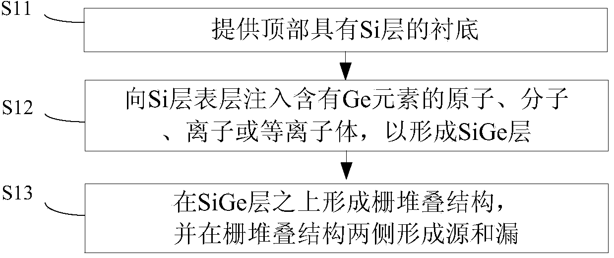
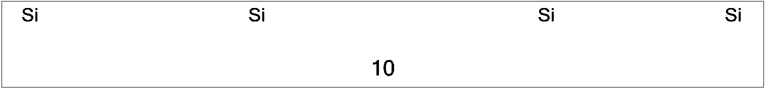
[0034] Embodiments of the present invention are described in detail below, examples of which are shown in the drawings, wherein the same or similar reference numerals designate the same or similar elements or elements having the same or similar functions throughout. The embodiments described below by referring to the figures are exemplary and are intended to explain the present invention and should not be construed as limiting the present invention.

[0035] In the present invention, unless otherwise clearly specified and limited, a first feature being "on" or "under" a second feature may include direct contact between the first and second features, and may also include the first and second features Not in direct contact but through another characteristic contact between them. Moreover, "above", "above" and "above" the first feature on the second feature include that the first feature is directly above and obliquely above the second feature, or simply means that the first feat...


PUM

PropertyMeasurementUnit
Thicknessaaaaaaaaaa

Abstract

The invention provides an MOSFET with a SiGe channel and a forming method of the MOSFET. The forming method includes the following steps of providing a substrate with a Si layer at the top, injecting atoms, molecules, ions or plasmas containing Ge elements into the surface layer of the Si layer so that the SiGe layer can be formed, forming a gate stacking structure on the upper portion of the SiGe layer, and forming a source and a drain on the two sides of the gate stacking structure. According to the forming method of the MOSFET, the MOSFET with the SiGe channel can be formed, the SiGe channel is thin, crystalline quality is good, and accordingly the MOSFET has good electrical property and the method has the advantages of being simple, easy to carry out and low in cost.

Description

technical field [0001] The invention relates to the field of semiconductor manufacturing, in particular to a MOSFET with a SiGe channel and a forming method thereof. Background technique [0002] With the development of microelectronics technology and the continuous reduction of MOSFET device size, the low mobility of Si material has become the main factor restricting device performance. In order to continuously improve the performance of the device, measures must be taken to increase the carrier mobility in the channel. At present, the strained silicon technology is widely used in the industry. Since strained SiGe has a higher mobility than Si, strained SiGe channel technology can be used for MOSFETs, that is, strained SiGe materials are used in the channel region to improve the electrical performance of MOSFET devices. [0003] When growing SiGe materials, the commonly used method is chemical vapor deposition (CVD) process, which is complex and difficult to control the qu...

Claims


Application Information

Patent Timeline
IPC IPC(8): H01L21/336H01L21/265H01L29/78H01L29/10
CPCH01L29/78H01L21/26513H01L29/1033H01L29/4232H01L29/66477
Inventor 王敬肖磊梁仁荣许军
Owner TSINGHUA UNIV
Why Eureka
Try Eureka