Embedded touch colour-film substrate and manufacturing method thereof

A technology of color film substrate and manufacturing method, applied in the field of flat panel display, capable of solving problems such as long coating time

Active Publication Date: 2014-08-13
SHANGHAI TIANMA MICRO ELECTRONICS CO LTD +1
View PDF3 Cites 5 Cited by
  • Summary
  • Abstract
  • Description
  • Claims
  • Application Information

AI Technical Summary

Problems solved by technology

In order to save production time, different coating speeds will be used for the sealant 104 and the conduction sealant 114. Because the coating accuracy of

Method used


Image

  • Embedded touch colour-film substrate and manufacturing method thereof
  • Embedded touch colour-film substrate and manufacturing method thereof
  • Embedded touch colour-film substrate and manufacturing method thereof

Examples


no. 1 example

[0063] see Figure 2-Figure 12 The first embodiment of the present invention will be specifically described.

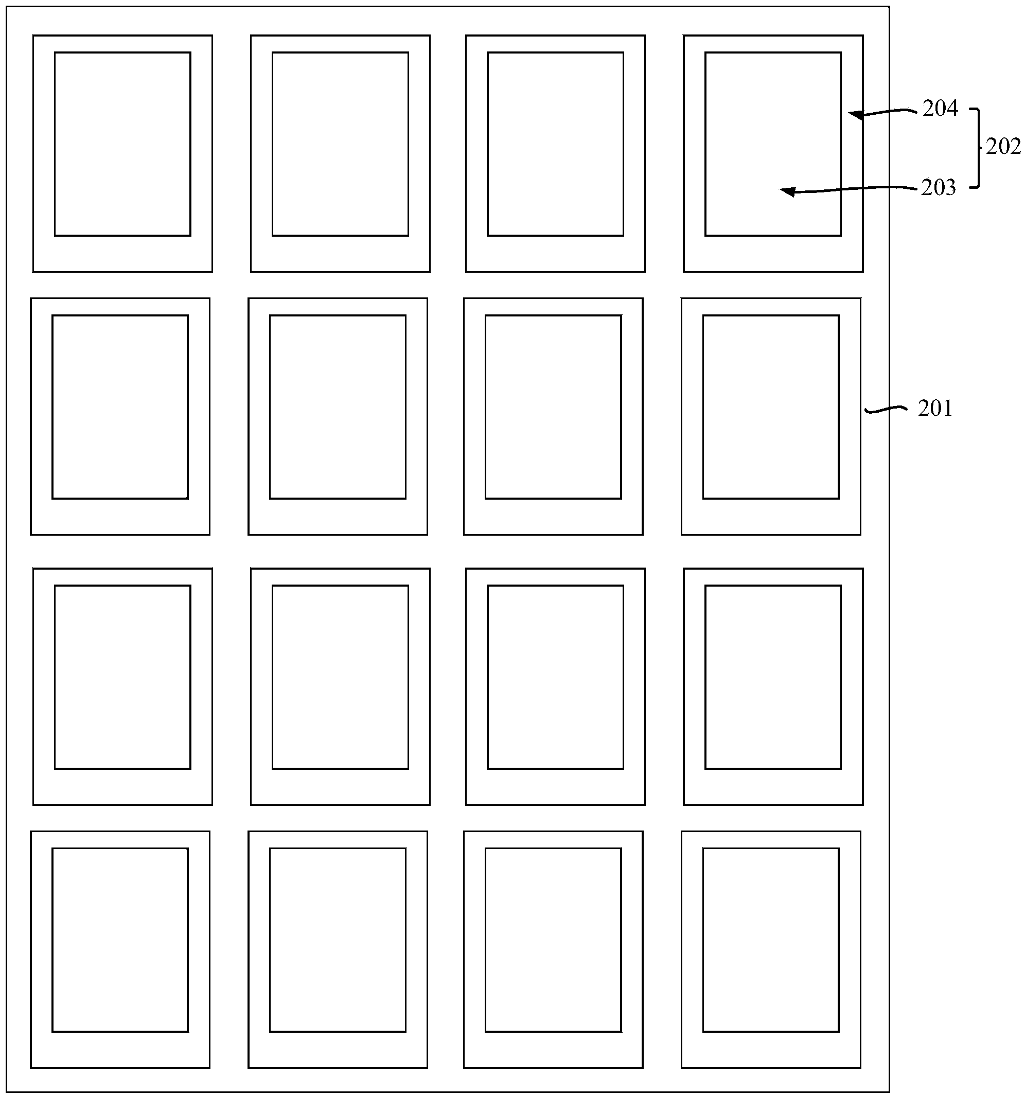
[0064] First, if figure 2 As shown, a substrate 201 is provided, and the substrate 201 includes a plurality of display units 202 , and each display unit 202 includes a display area 203 and a plurality of non-display areas 204 surrounding the display area 203 . Each of the display units 202 corresponds to a subsequent embedded touch display screen. For the convenience of description, one display unit is used as an example for illustration below.

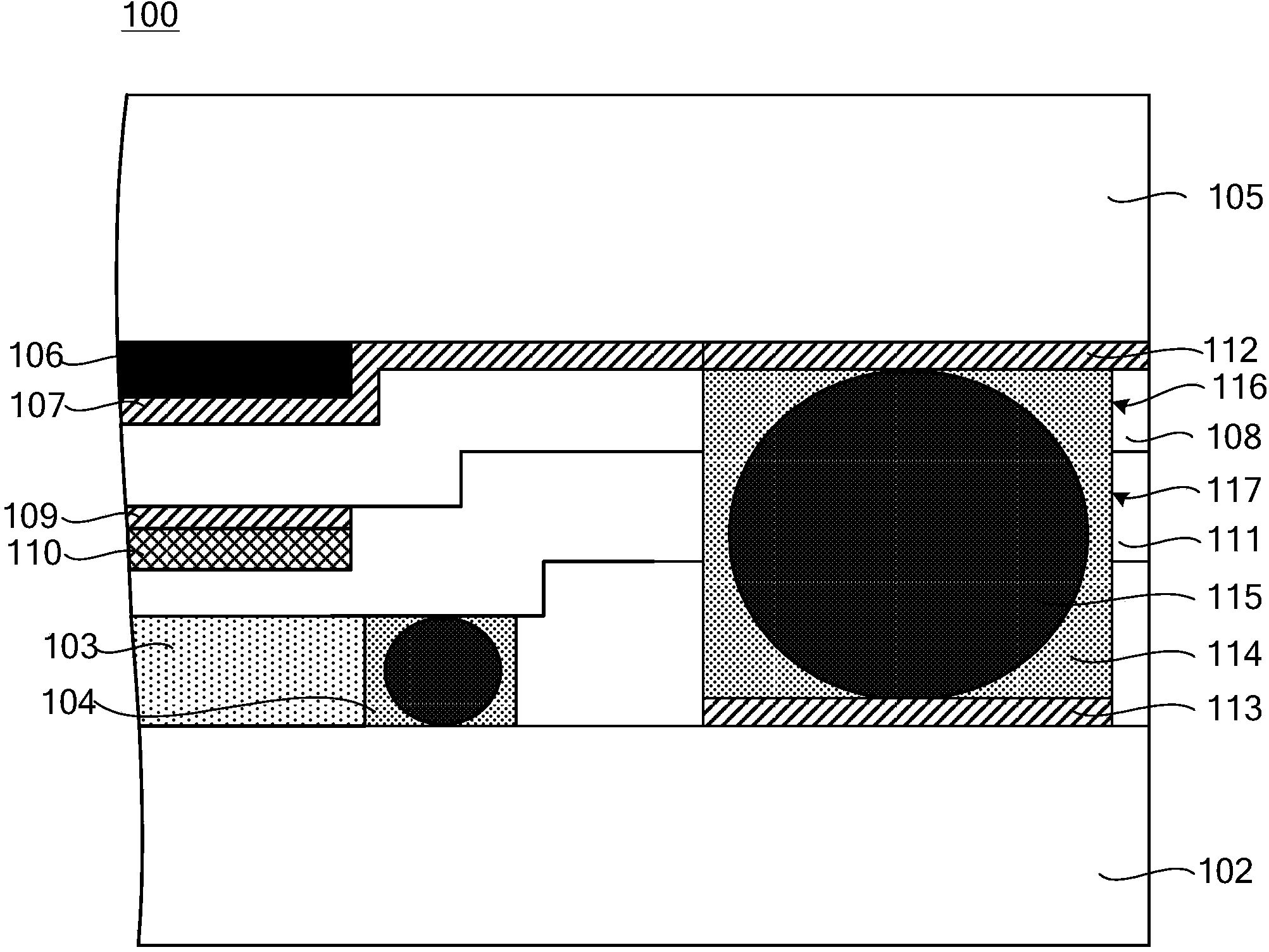
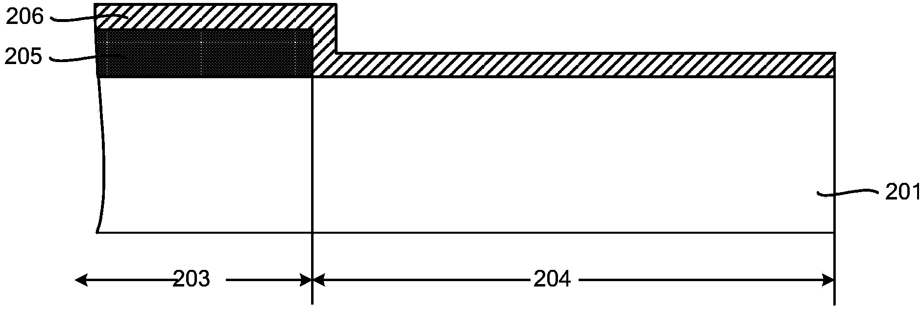
[0065] Such as image 3 As shown, a black matrix 205 and a first metal layer 206 are sequentially formed on the substrate 201 , and the black matrix 205 is only formed in the display area 203 . In the present invention, the first metal layer 206 is used as a driving electrode or a scanning electrode to complete the touch function, and the first metal layer 206 located in the display area 203 is a mesh structure formed on ...

no. 2 example

[0078] see Figure 13-Figure 16 , Figure 13 It is a schematic structural diagram of the display unit in the embedded touch screen according to the second embodiment of the present invention; Figure 14 for Figure 13 Partial sectional view along line AA'; Figure 15 It is a schematic diagram of the structure of the pad area in Embodiment 2 of the present invention; Figure 16 It is a cross-sectional view of the in-cell touch color filter substrate after the application of the frame sealant in the second embodiment of the present invention. exist Figure 13-Figure 16 , the reference numerals indicate the same Figure 2-Figure 12 The same expressions are the same components as those of the first embodiment. The in-cell touch color filter substrate 600 of the second embodiment is basically the same as the in-cell touch color filter substrate 200 of the first embodiment, the difference is that there are several pad areas in the non-display area, There are several conductiv...


PUM

PropertyMeasurementUnit
Thicknessaaaaaaaaaa
Diameteraaaaaaaaaa

Abstract

The invention discloses an embedded touch colour-film substrate and a manufacturing method thereof. The embedded touch colour-film substrate comprises a substrate, first metal layers, first organic film layers, second metal layers and second organic film layers, wherein the substrate comprises multiple display areas and multiple nondisplay areas surrounding the display areas; the first metal layers, the first organic film layers, the second metal layers and the second organic film layers are formed on the substrate in sequence; each of the second metal layers comprises multiple electric conduction cushions arranged in the nondisplay areas; multiple through holes or through grooves are formed in each of the first organic film layers in the nondisplay areas; the electric conduction cushions are respectively and electrically connected with the first metal layers through the through holes or the through grooves; moreover, the electric conduction cushions are respectively exposed outside the second organic film layers. By applying the embedded touch colour-film substrate provided by the invention, the time on coating a frame sealing glue can be effectively shortened, so that the production efficiency can be improved greatly.

Description

technical field [0001] The invention relates to flat panel display technology, in particular to an embedded touch screen color filter substrate and a manufacturing method thereof. Background technique [0002] The touch screen embedded in the liquid crystal display is widely used because it can be integrated with the color filter substrate, which can effectively reduce the thickness of the entire touch display device and simplify the manufacturing process. Usually, the mutual capacitance is composed of two layers of metal integrated on the color filter substrate and a layer of organic film, and the touch monitoring is completed by detecting the capacitance value of the mutual capacitance. The transmission of the touch detection signal is conducted to the color filter substrate through the gold ball on the array substrate through the conductive pad. [0003] Specifically, if figure 1 As shown, the in-cell touch screen 100 in the prior art includes: an in-cell touch color fi...

Claims


Application Information

Patent Timeline
IPC IPC(8): G02F1/1335G02F1/1345G02F1/1339G02F1/1333G06F3/041
Inventor 赵丽军马骏
Owner SHANGHAI TIANMA MICRO ELECTRONICS CO LTD
Why Eureka
Try Eureka