Check patentability & draft patents in minutes with Patsnap Eureka AI!

NAND flash memory structure logic MTP compatible with CMOS technology

A flash memory and process technology, applied in the field of integrated circuits, can solve problems such as high process cost, long R&D cycle, and incompatibility of CMOS logic process, and achieve the effect of reducing bit area and cost

Active Publication Date: 2014-08-27
SUZHOU FENGCHI MICROELECTRONICS
View PDF5 Cites 0 Cited by
  • Summary
  • Abstract
  • Description
  • Claims
  • Application Information

AI Technical Summary

Problems solved by technology

Usually non-volatile memory is required to store data, ID, etc., but the usual embedded Flash requires a special process and high cost, the development cycle is long, and it is not compatible with the usual CMOS logic process

Method used


Image

  • NAND flash memory structure logic MTP compatible with CMOS technology
  • NAND flash memory structure logic MTP compatible with CMOS technology
  • NAND flash memory structure logic MTP compatible with CMOS technology

Examples


Embodiment Construction

[0013] The present invention will be further described below in conjunction with drawings and embodiments.

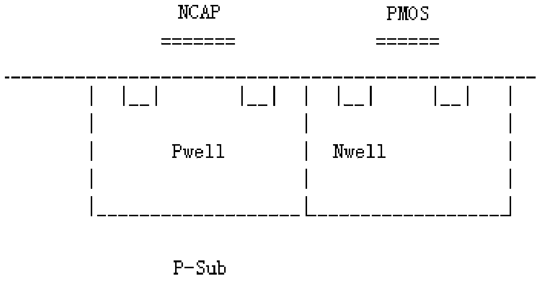
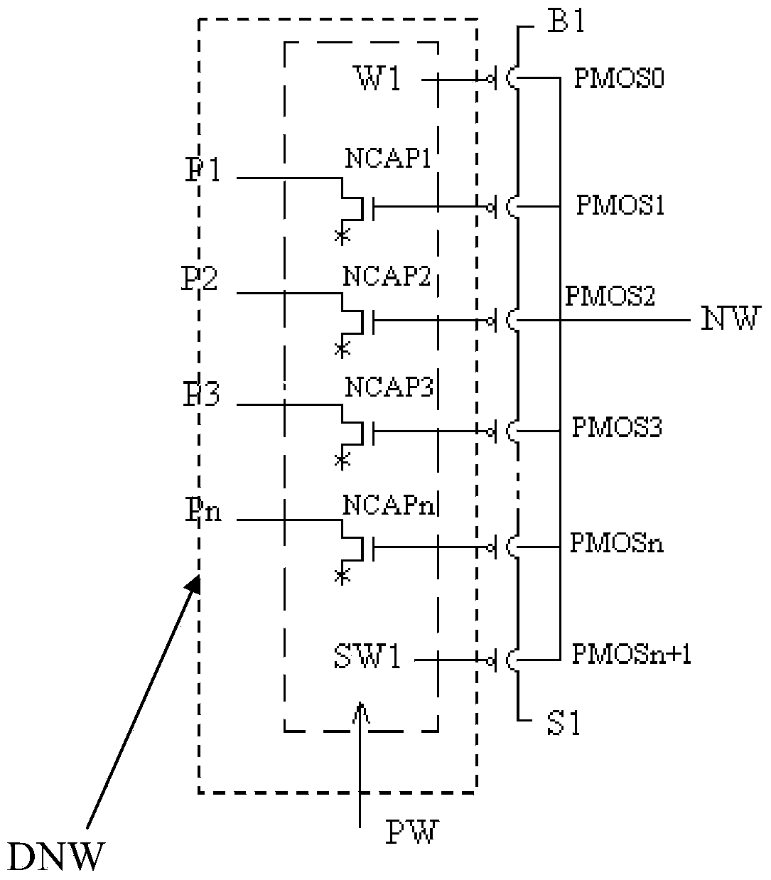
[0014] The logical MTP of the NAND flash memory structure of the present invention comprises: a PMOS transistor and an NCAP (NMOS is done in the N well) capacitance composition unit, wherein the NCAP capacitance has a floating gate, the drain of the NCAP capacitance is connected to the programming line, and the NCAP capacitance The floating gate is connected to the gate of the PMOS transistor; as figure 1 NCAP1 and PMOS1 constitute units in NCAP2 and PMOS2 constitute units, and so on. The drains of the NCAP capacitors NCAP1 , NCAP2 , . . . , NCAPn are respectively connected to programming lines P1 , P2 , . . . Pn. Then 2 or more such cells are combined in series, that is, the drain of each PMOS transistor is connected to the source of the next PMOS transistor, such as figure 1 PMOS1, PMOS2, . . . , PMOSn connected in series. The source of the first PMOS transistor PM...


PUM


Abstract

The invention relates to an NAND flash memory structure logic MTP compatible with the CMOS technology. The NAND flash memory structure logic MTP comprises a PMOS transistor and a unit composed of an NCAP capacitor, wherein a drain electrode of the NCAP capacitor is connected with a programming line, and a floating gate of the NCAP capacitor is connected with a grid electrode of the PMOS transistor. Then, two or more units are combined together in a serial-connecting mode, and in other words, a drain electrode of each PMOS transistor is connected with a source electrode of the next PMOS transistor; the PMOS transistors which are connected in series end to end are further respectively connected with one PMOS transistor in series, substrates of all the PMOS transistors are connected together through an N trap, and substrates of all the NCAP capacitors are connected together through a P trap. The P trap can be or not be made in the deep N trap, and the P trap and a p-type substrate in the deep N trap are separated through the deep N trap. The NAND flash memory structure logic MTP compatible with the CMOS technology has the advantages that the PMOS transistors and the basic unit composed of the NCAP capacitors are connected in series so that the storage function can be achieved, connection between the source electrode and the drain electrode of each PMOS transistor can be omitted, the bit area of each basic unit is greatly reduced, and cost is reduced.

Description

technical field [0001] The invention relates to a non-volatile memory, in particular to a non-volatile memory compatible with CMOS logic technology, and belongs to the technical field of integrated circuits. Background technique [0002] For system-on-chip (SoC) applications, many blocks with different functions are integrated into one integrated circuit. Usually non-volatile memory is required to store data, ID, etc., but the usual embedded Flash requires a special process and high cost, the development cycle is long, and it is not compatible with the usual CMOS logic process. Contents of the invention [0003] The purpose of the present invention is to overcome the deficiencies in the prior art, to provide a logic MTP with a NAND flash memory structure compatible with the CMOS process, which can reduce costs, has a small single bit area, and is fully compatible with traditional semiconductor processes and CMOS logic processes . [0004] According to the technical solut...

Claims


Application Information

Patent Timeline
Patent Type & Authority Applications(China)
IPC IPC(8): H01L27/115G11C16/02H10B69/00
Inventor 方钢锋
Owner SUZHOU FENGCHI MICROELECTRONICS
Features
  • R&D
  • Intellectual Property
  • Life Sciences
  • Materials
  • Tech Scout
  • Unparalleled Data Quality
  • Higher Quality Content
  • 60% Fewer Hallucinations
Learn More