White LED chip and manufacturing method thereof

A technology of LED chip and manufacturing method, which is applied in the direction of electrical components, circuits, semiconductor devices, etc., can solve the problems of easy-to-contaminate LED chips, poor welding of white LED chips, and light leakage of LED chips, so as to improve luminous efficiency and avoid easy production and processing , The effect of high product yield

Active Publication Date: 2014-09-03
APT ELECTRONICS
View PDF7 Cites 15 Cited by
  • Summary
  • Abstract
  • Description
  • Claims
  • Application Information

AI Technical Summary

Problems solved by technology

[0004] The purpose of the present invention is to provide a method for manufacturing white LED chips and the LED chips manufactured by the method, so as to solve the problem of poor welding and LED chip side which are easy to pollute the electrodes of LED chips in the existing manufacturing process and affect the subsequent process of white LED chips. light leak problem

Method used


Image

  • White LED chip and manufacturing method thereof
  • White LED chip and manufacturing method thereof
  • White LED chip and manufacturing method thereof

Examples


Embodiment 1

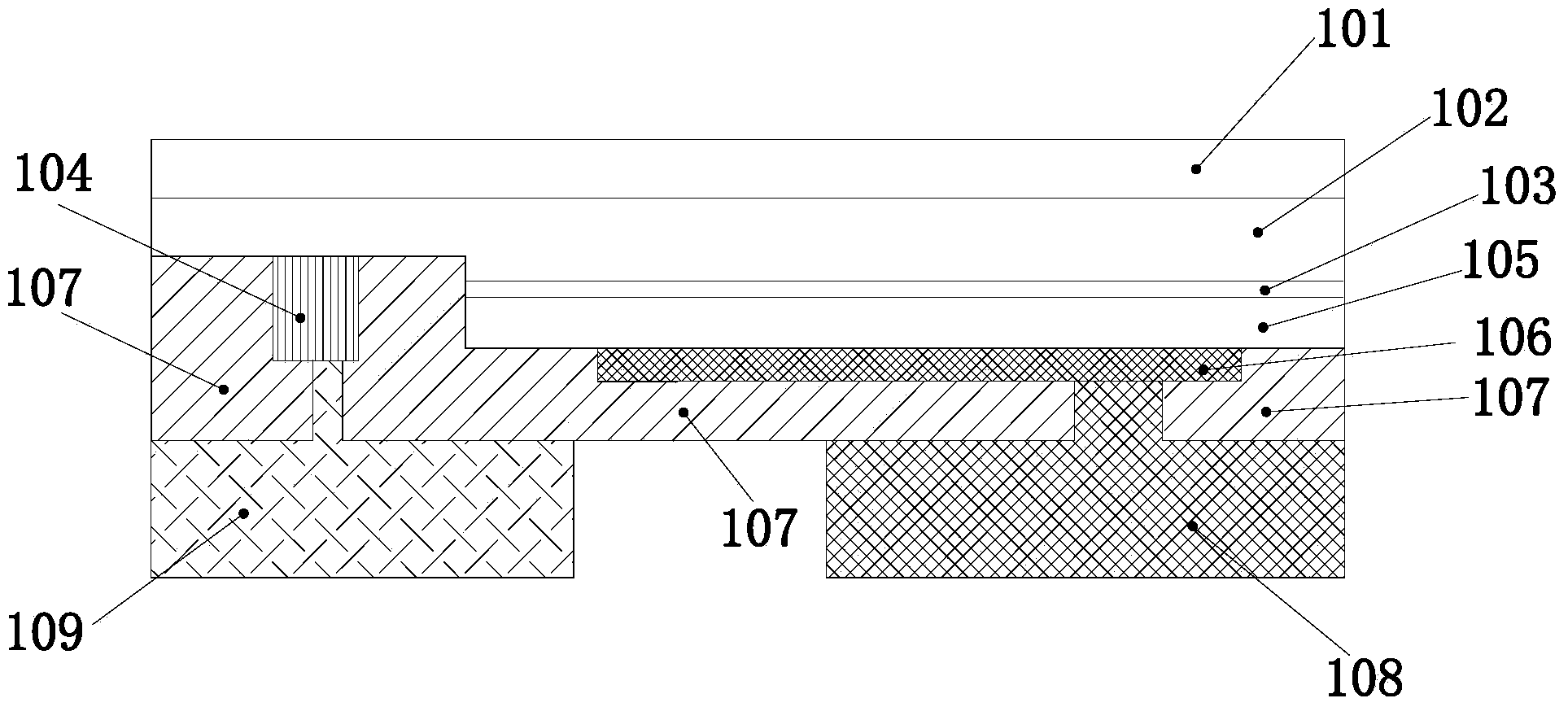
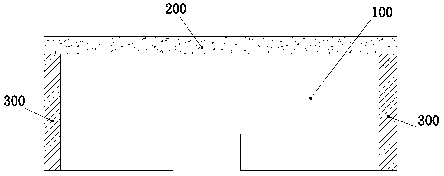
[0044] Such as figure 2 As shown, this embodiment discloses a white light LED chip, including a mounted LED chip 100, on the epitaxial substrate layer of the mounted LED chip 100, prefabricated light for light color conversion is mounted. The conversion layer sheet 200 is closely surrounded by a reflective wall 300 for preventing light leakage from the side of the LED chip around the mountable LED chip 100 , and the reflective wall 300 is connected to the light conversion layer sheet 100 .

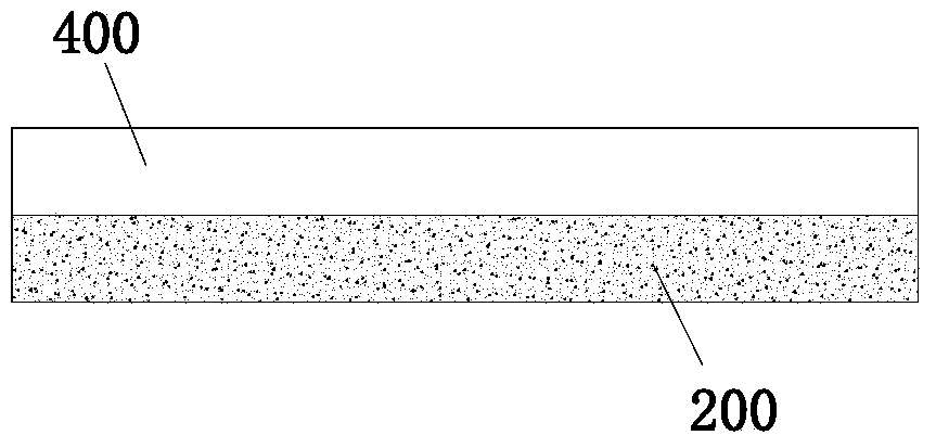
[0045]Wherein, the light conversion layer sheet 200 is a prefabricated sheet-shaped material, and the light conversion layer sheet 200 is used to convert light color. For example, when the mounted LED chip 100 is a blue LED chip, the light conversion layer sheet 200 is selected. Yellow light conversion material, so as to convert blue light into white light. It should be noted that this patent is not limited to blue light LED chips and yellow light conversion materials. Other situations th...

Embodiment 2

[0058] Figure 4a- Figure 4c As shown, the difference between this embodiment and Embodiment 1 is that the (1) step of the manufacturing method of the white light LED chip of this embodiment is specifically as follows: the pre-prepared block-shaped reflective wall 300 is bonded to the light The surface of the conversion layer sheet 200 encloses a plurality of LED chip installation cavities.

[0059] In this embodiment, the process of making a white LED chip is specifically as follows:

[0060] 1. If Figure 4a1 As shown, now the pre-prepared block-shaped reflective wall 300 is bonded on the surface of the light conversion layer sheet 200, Figure 4a1 is a sectional view, Figure 4a2 It is a top view after bonding. It can be seen from the figure that the reflective wall 300 forms a plurality of LED installation cavities for installing LED chips on the surface of the light conversion layer sheet 200 .

[0061] 2. If Figure 4b As shown, then mount the mount-type LED chip 10...

Embodiment 3

[0063] This embodiment is also slightly different from Embodiment 1. This embodiment discloses a method for manufacturing a white light LED chip, which specifically includes the following steps:

[0064] (1), such as Figure 5a As shown, the LED chip 100 is first mounted on the surface of the prefabricated light conversion layer sheet 200;

[0065] (2), such as Figure 5b As shown, a layer of polymer reflective material is coated on the light conversion layer sheet 200 pasted with the LED chip 100 and cured, and the polymer reflective material completely covers the LED chip;

[0066] (3), such as Figure 5c As shown, the polymer reflective material on the upper surface is ground to expose the electrodes of the LED chip, and it is cut into a single white LED chip with a light conversion layer on the top and a reflective wall around it, Figure 5d It is the final single white LED chip.

[0067] In this embodiment, the LED chip 100 is first mounted on the surface of the prefa...


PUM


Abstract

The invention discloses a white LED chip and a manufacturing method thereof. The white LED chip comprises a mount type LED chip. A pre-molded optical conversion layer slice for light color conversion is mounted on an epitaxial substrate layer of the mount type LED chip. A light reflecting walls for light leakage at side surfaces of the LED chip closely surrounds the periphery of the mount type LED chip. The light reflecting wall is connected with the optical conversion layer slice. The manufacturing method of the while LED chip comprises the following steps: (1) manufacturing the light reflecting wall on the surface of the optical conversion layer slice, wherein the light reflecting wall is provided with a plurality of LED chip mounting chambers on the surface of the optical conversion layer slice; and (2) mounting the mount type LED chip in the LED mount chamber, and cutting the mount type LED chip to a single white LED chip which is provided with an optical conversion layer on the upper part and is provided with the light reflecting wall at the periphery. The white LED chip can improve light emitting efficiency of the white LED chip and furthermore can prevent bottom electrode pollution of the LED chip according to the prior art. Furthermore the white LED chip has advantages of easy production and high yield of the product.

Description

technical field [0001] The invention belongs to the technical field of LEDs, and in particular relates to a white LED chip and a manufacturing method thereof. Background technique [0002] White light LED chips are LED chips that can directly emit white light using Chip Scale Package (hereinafter referred to as "CSP") technology. This type of chip has the advantages of small size, large luminous angle, high current drive resistance, low manufacturing cost, and convenient downstream. Customer lighting design. [0003] The common structural features of current LED white light chips: flip-chip structure, the electrodes are at the bottom, and the top and four sides are covered with phosphor. The phosphor layer directly above and on the four sides is generally realized by molding and pressing semi-cured phosphor sheet technology, and the phosphor layer directly above and on the four sides is an integrally formed structure of the same material. Another example is Chinese Patent ...

Claims


Application Information

Patent Timeline
Patent Type & Authority Applications(China)
IPC IPC(8): H01L33/48H01L33/60H01L33/50
CPCH01L33/486H01L33/50H01L33/60H01L2933/0058
Inventor 万垂铭许朝军姜志荣姚述光曾照明肖国伟
Owner APT ELECTRONICS
Why Eureka
Try Eureka