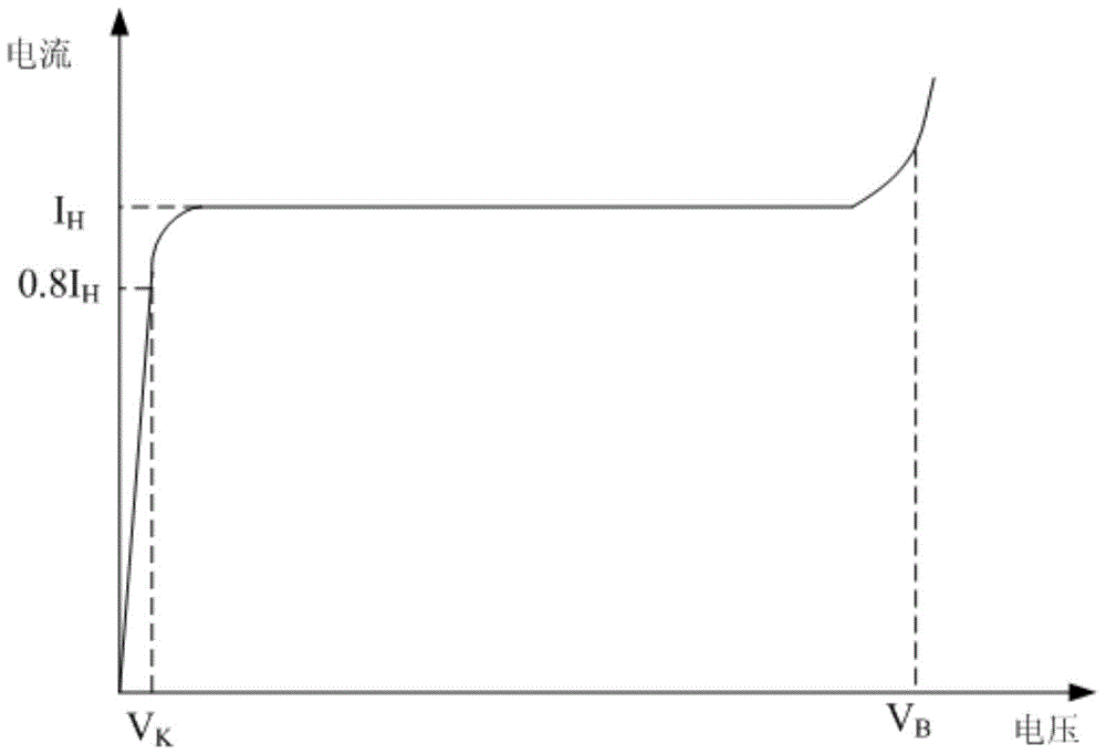
A two-terminal constant current device
A constant-current device, depletion-mode transistor technology, applied in instruments, regulating electrical variables, control/regulating systems, etc., can solve the problems of poor temperature stability, narrow constant current region, low breakdown voltage, etc., to achieve temperature stability High, fast response, high breakdown voltage effect
- Summary
- Abstract
- Description
- Claims
- Application Information
AI Technical Summary
Problems solved by technology
Method used
Image
Examples
Embodiment 1
[0028] figure 1 It is a schematic diagram of a two-terminal constant current device provided in Embodiment 1 of the present invention, see figure 1 . The two-terminal constant current device includes: a first N-type depletion transistor T1 and a resistor R, wherein the source of the first N-type depletion transistor is connected to the first end of the resistor R, and the first The gate of an N-type depletion transistor T1 is connected to the second end of the resistor R, wherein the first N-type depletion transistor T1 is a gallium nitride depletion transistor, and the resistor R is separated resistor or a resistor integrated with the first N-depletion transistor T1.
[0029] In this embodiment, the two-terminal constant current device further includes a first-type electrode and a second-type electrode. Wherein, the first-type electrode is the anode PP of the two-terminal constant current device, the drain of the first N-type depletion transistor T1 is used as the anode PP...
Embodiment 2
[0044] image 3 It is a schematic diagram of a two-terminal constant current device provided in Embodiment 2 of the present invention. This embodiment is based on Embodiment 1, see image 3 , the two-terminal constant current device includes a first N-type depletion transistor T1, a second N-type depletion transistor T2 and a resistor R, wherein the drain of the second N-type depletion transistor T2 is connected to the The source of the first N-type depletion transistor T1 is connected, the source of the second N-type depletion transistor T2 is connected to the first end of the resistor R, and the second N-type depletion transistor T2 The gate of the gate is connected to the gate of the first N-type depletion transistor T1 and then connected to the second end of the resistor R. Wherein, the first N-type depletion transistor T1 and the second N-type depletion transistor T2 are gallium nitride depletion transistors, and the resistor R is a separate resistor or connected with t...
Embodiment 3
[0054] Figure 4 It is a schematic diagram of a two-terminal constant current device provided by Embodiment 3 of the present invention. This embodiment is based on the above-mentioned embodiment, see Figure 4 , the two-terminal constant current device includes a first N-type depletion transistor T1, a second N-type depletion transistor T2 and a resistor R. Wherein, the second N-type depletion transistor T2 is composed of N third N-type depletion transistors T3. The third N-type depletion transistor T3 is a gallium nitride depletion transistor, wherein N is an integer greater than or equal to 2.
[0055] The gates of the N third N-type depletion transistors T3 are connected together as the gates of the second N-type depletion transistor T2, and the gates of the first third N-type depletion transistor T31 The drain serves as the drain of the second N-type depletion transistor T2, and the drain of each third N-type depletion transistor T3 is connected to the source of the pre...
PUM
 Abstract
Description
Claims
Application Information


