Chip stripping device and system and device for controlling chip stripping

A technology for stripping devices and wafers, which is applied in semiconductor/solid-state device manufacturing, semiconductor devices, electrical components, etc. It can solve problems such as high production costs and damage to wafer quality, and achieve the effect of improving production efficiency

Active Publication Date: 2014-09-17
威科赛乐微电子股份有限公司
View PDF7 Cites 6 Cited by
  • Summary
  • Abstract
  • Description
  • Claims
  • Application Information

AI Technical Summary

Problems solved by technology

[0005] Embodiments of the present invention provide a wafer stripping device, a system, and a device for controlling wafer stripping, which realizes the automatic design of semiconductor wafer stripping technology after polishing, and solves the problem of poor wafer quality caused by manual misoperation in the prior art. technical problems of loss and high production cost, thereby further improving the production efficiency of semiconductor materials

Method used


Image

  • Chip stripping device and system and device for controlling chip stripping
  • Chip stripping device and system and device for controlling chip stripping
  • Chip stripping device and system and device for controlling chip stripping

Examples


no. 1 example

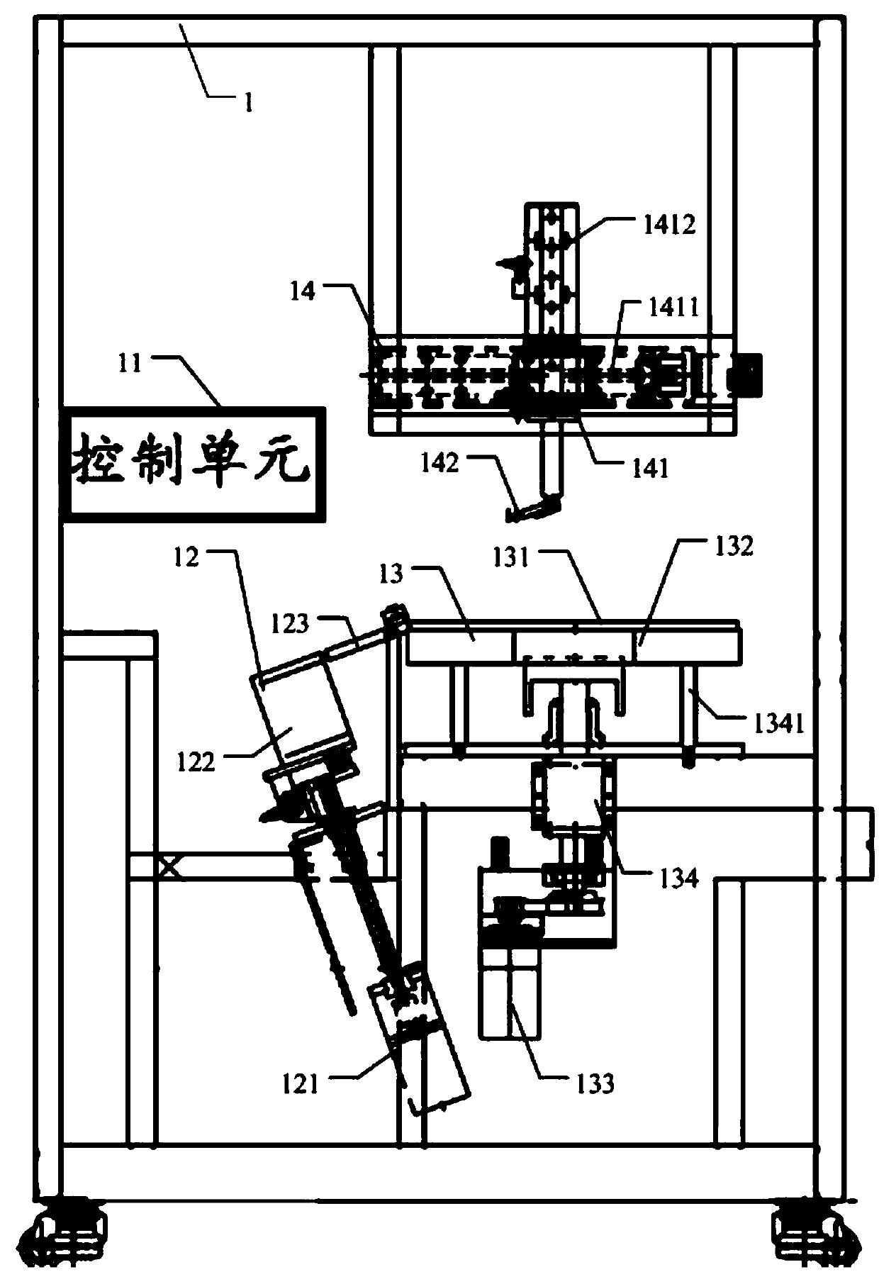
[0065] see figure 1 , the first embodiment of a wafer peeling device provided by the embodiment of the present invention includes:

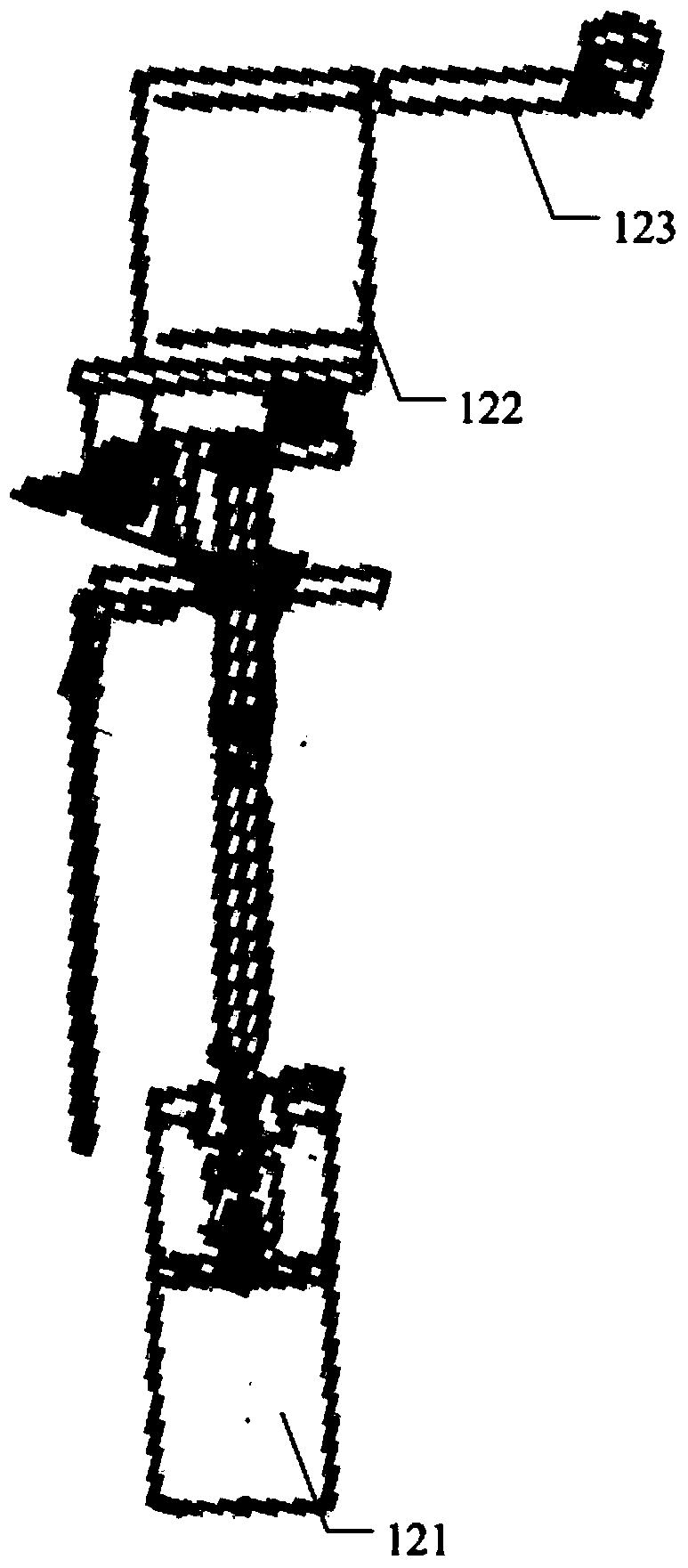
[0066] Control unit 11, wafer pick-up unit 12, heating unit 13 and stripping unit 14, control unit 11 is connected with wafer pick-up unit 12, heating unit 13 and stripping unit 14 by connecting wire, control unit 11 is used for sending control command, wafer pick-up The unit 12, the heating unit 13 and the peeling unit 14 perform operations corresponding to the control instructions;

[0067] It can be understood that, the wafer peeling process of a wafer peeling device 1 provided in the embodiment of the present invention may be that the control unit 11 controls the heating unit 13 to heat the wafer, and when the wafer heating is completed, the control unit 11 controls the peeling unit 14 to The wafers on the heating unit 13 are transferred to the wafer transfer unit 12 .

[0068] It must be noted that the aforementioned wafer stripping proces...

no. 3 example

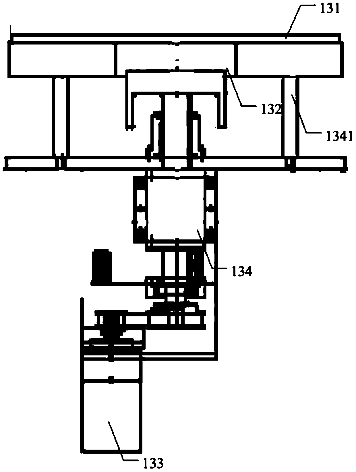
[0079] see figure 1 with image 3 , a third embodiment of a wafer peeling device provided in an embodiment of the present invention includes:

[0080] As mentioned above, the heating unit 13 includes a ceramic disc 131, a heating component 132, a second motor 133 and a rotating component 134. The heating component 132 is installed at the bottom of the ceramic disc 131. It should be noted that there is a groove in the middle of the ceramic disc 131, so that the heating component 132 During the heating process, heating is carried out from the middle of the ceramic plate 131 to the outer edge. The heating part 132 is a heat conduction shell with an electric heating wire installed inside. The heat conduction shell is a semi-closed ceramic aluminum alloy shell. In the aluminum alloy casing, the second motor 133 is connected to the rotating part 134, and is used to rotate the rotating part 134 in the horizontal direction by 360° through electric energy. The rotating part 134 also i...

no. 4 example

[0082] The specific structure of the stripping unit 14 and the process in which the stripping unit 14 performs wafer stripping according to the preset stripping mode will be described in detail below, please refer to figure 1 with Figure 4 , the fourth embodiment of a wafer peeling device provided by an embodiment of the present invention includes:

[0083] Aforesaid stripping unit 14 comprises: moving subunit 141 and blade 142, and moving subunit 141 comprises horizontal operating arm 1411 and vertical operating arm 1412, and horizontal operating arm 1411 and vertical operating arm 1412 are connected in a cross shape, and the edge of blade 142 is The tooth structure is installed on the bottom of the vertical operating arm 1412. The material of the aforementioned blade 142 can be resin material. It must be noted that the blade 142 is connected to the vertical operating arm 1412 at a certain angle, and the angle can be greater than 90° For example, when a plurality of wafers ...


PUM


Abstract

The embodiment of the invention discloses a chip stripping device and system and a device for controlling chip stripping. The chip stripping device and system and the device for controlling chip stripping achieve the automatic design of the technology that a semiconductor chip is polished and then stripped, resolve the technical problems that due to manual misoperation in the prior art, the quality of the chip is damaged, and the production cost is high, and further improve the production efficiency of semiconductor materials. The chip stripping device comprises a control unit, a chip receiving and conveying unit, a heating unit and a stripping unit, wherein the control unit is connected with the chip receiving and conveying unit, the heating unit and the stripping unit through connecting lines, the control unit is used for sending a control instruction to the chip receiving and conveying unit, the heating unit and the stripping unit execute operation corresponding to the control instruction, and the control unit controls the heating unit to heat the chip and controls the stripping unit to convey the chip on the heating unit to the chip receiving and conveying unit after the chip is heated.

Description

technical field [0001] The invention relates to the field of mechanical equipment, in particular to a wafer stripping device, a system and a device for controlling wafer stripping. Background technique [0002] With the rapid development of science and technology, semiconductor materials are widely used in high-tech technologies, such as chip preparation, etc. Therefore, the preparation technology of semiconductor materials has also attracted much attention, especially for the preparation of semiconductor wafers, which require high-precision cutting, grinding and polishing. And other processing technology for processing. [0003] In the existing technology for peeling off polished wafers, in the semiconductor wafer production industry, the current processing method for those skilled in the art is usually to use simple heating equipment, and then use the peeling method of manual shovel technology. For semiconductor wafers, for example, place a ceramic plate with a polished w...

Claims


Application Information

Patent Timeline
Patent Type & Authority Applications(China)
IPC IPC(8): H01L21/67
CPCH01L21/67103H01L21/67248H01L21/67253H01L24/799
Inventor 朱刘刘留
Owner 威科赛乐微电子股份有限公司
Why Eureka
Try Eureka