
Array substrate, manufacturing method thereof, and display device

A technology of array substrates and substrate substrates, which is applied in semiconductor/solid-state device manufacturing, optics, instruments, etc., can solve problems affecting product yield and achieve the effect of avoiding ESD phenomena

Active Publication Date: 2017-06-23
BOE TECH GRP CO LTD +1
View PDF2 Cites 0 Cited by
  • Summary
  • Abstract
  • Description
  • Claims
  • Application Information

AI Technical Summary

Problems solved by technology

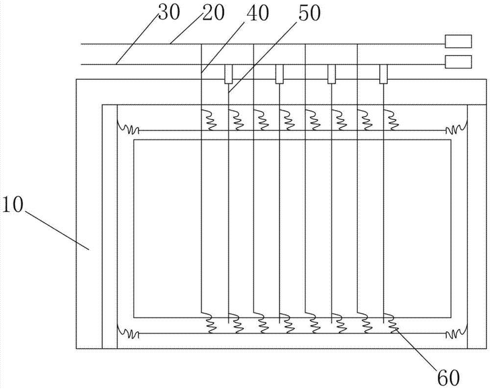
[0005] Although the ESD protection device 60 is connected to the data line, the ESD protection device includes a plurality of TFTs, the source of the TFT is connected to the data line, and its drain is connected to the third short-circuit line, and the source and the gate need to be connected by ITO. ITO is generally deposited in the last step. Since the data line is a long metal line, it is easy to accumulate static electricity during the sputtering and etching process of the data line, and these static electricity cannot be released through the ESD protection device before ITO deposition. Therefore, the ESD phenomenon is likely to occur in the overlapping area of ​​the above-mentioned data lines, which affects the yield of the product

Method used


Image

  • Array substrate, manufacturing method thereof, and display device
  • Array substrate, manufacturing method thereof, and display device

Examples


Embodiment Construction

[0031] The specific implementation manners of the present invention will be further described in detail below in conjunction with the accompanying drawings and embodiments. The following examples are used to illustrate the present invention, but are not intended to limit the scope of the present invention.

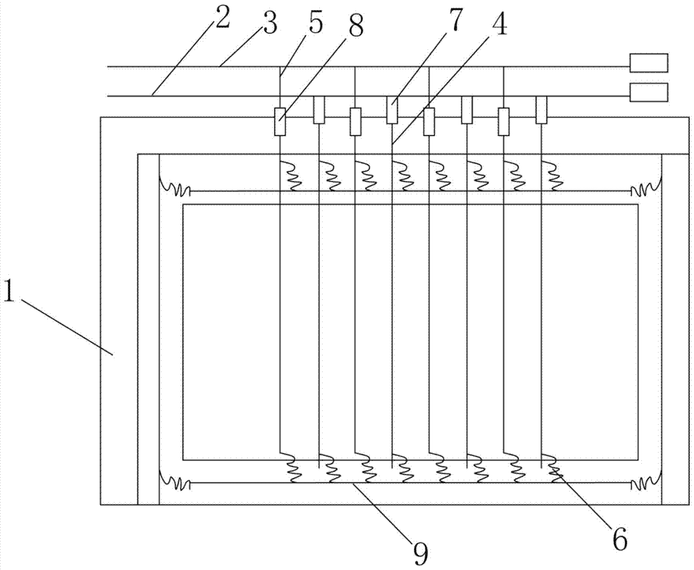
[0032] For the convenience of testing, in the TFT-LCD manufacturing process, it is necessary to check the wiring on the array substrate. Therefore, in order to facilitate the wiring inspection, the data lines of the array substrate are generally divided into two groups of odd and even, and each group is connected to a different short circuit, such as figure 2 As shown, an array substrate of the present invention includes a base substrate 1, a first short circuit 2, a first insulating layer, a data line and a second insulating layer sequentially formed on the base substrate 1 from bottom to top. , the layer where the data line is located is formed with a second short-circu...


PUM


Abstract

The invention relates to the field of display techniques and discloses an array substrate and a manufacturing method and a display device thereof. The array substrate comprises a substrate body, a first short circuit wire, a first insulation layer, data lines and a second insulation layer, wherein the first short circuit wire, the first insulation layer, the data lines and the second insulation layer are sequentially formed on the substrate body from bottom to top, a second short circuit wire is formed in a layer where the data lines are located, the multiple data lines are divided into a first data line unit and a second data line unit, each data line is connected with an ESD protective device, the data lines of the second data line unit are connected with the second short circuit wire, and a second conductive wire penetrates through a via hole of the second insulation layer to be connected with two sections of data lines of the second data line unit. A first conductive line penetrates through a via hole of the first insulation layer and the via hole of the second insulation layer to be connected with the data lines of the first data line unit and the first short circuit wire. The array substrate can avoid the ESD phenomenon happening in a data line intersecting area in the manufacturing process of the array substrate, and accumulated static is finally released through the ESD protective device.

Description

technical field [0001] The present invention relates to the field of display technology, in particular to an array substrate, a method for preparing and wiring the same, and a display device. Background technique [0002] Electro-Static discharge (ESD, Electro-Static discharge) phenomenon is one of the main unfavorable phenomena of the array substrate process in the panel manufacturing process. Charge, in the process of charge transfer, encounters very thin traces or places where lines cross each other. Due to the excessive instantaneous current, ESD is prone to occur, which directly affects the yield of products. [0003] Thin Film Transistor-Liquid Crystal Display (TFT-LCD, Thin Film Transistor-Liquid Crystal Display) in the process of manufacturing, at the end of the array substrate preparation process, the inspection of the process needs to be carried out, which includes the disconnection and short-circuiting of metal wires and other defective inspections. [0004] In o...

Claims


Application Information

Patent Timeline
Patent Type & Authority Patents(China)
IPC IPC(8): H01L27/02H01L23/50H01L23/60H01L21/82G02F1/1362
Inventor 闫岩
Owner BOE TECH GRP CO LTD
Learn More