Array substrate and display device

A technology of array substrate and display area, applied in the direction of semiconductor devices, electrical components, circuits, etc., can solve problems such as easy occurrence of ESD, and achieve the effect of preventing ESD phenomenon, reducing the probability of ESD phenomenon, and reducing area difference

Active Publication Date: 2020-05-19
TCL CHINA STAR OPTOELECTRONICS TECH CO LTD
View PDF4 Cites 0 Cited by
  • Summary
  • Abstract
  • Description
  • Claims
  • Application Information

AI Technical Summary

Problems solved by technology

For the array substrate using GOA technology, the peripheral driving circuit is directly arranged on the array substrate. Due to the limitation of the wiring space, the wiring spacing in the first metal layer in the peripheral driving circuit is relatively small, while the first When the deposition method and dry etching process are used to prepare and form a patterned semiconductor layer on the metal layer, photogenerated carriers will be generated and accumulated on the surface of the semiconductor layer, and these photogenerated carriers will be directed toward the surface corresponding to the first metal layer. The traces in the center are gathered together, which is very prone to ESD phenomenon

Method used


Image

  • Array substrate and display device
  • Array substrate and display device
  • Array substrate and display device

Examples


Embodiment Construction

[0023] In order to make the object, technical solution and advantages of the present invention clearer, the specific implementation manners of the present invention will be described in detail below in conjunction with the accompanying drawings. Examples of these preferred embodiments are illustrated in the accompanying drawings. The embodiments of the invention shown in and described with reference to the drawings are merely exemplary, and the invention is not limited to these embodiments.

[0024] Here, it should also be noted that, in order to avoid obscuring the present invention due to unnecessary details, only the structures and / or processing steps closely related to the solution according to the present invention are shown in the drawings, and the related Other details are not relevant to the invention.

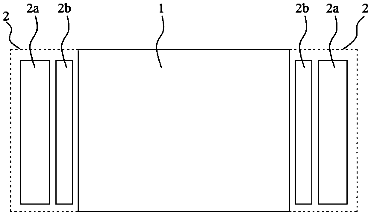
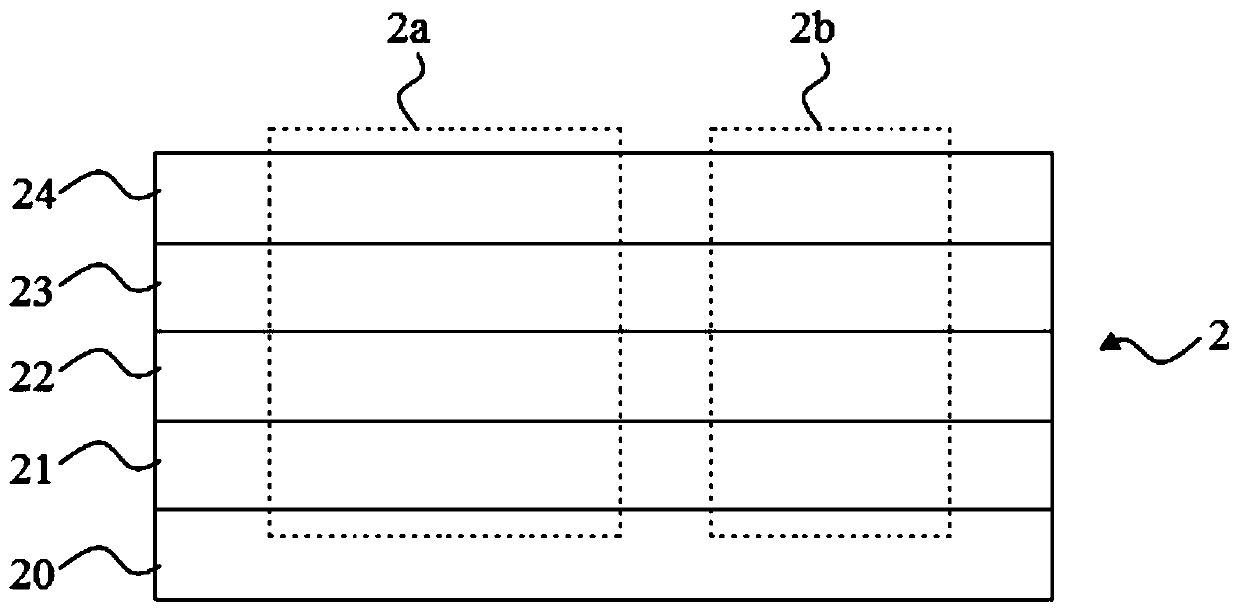
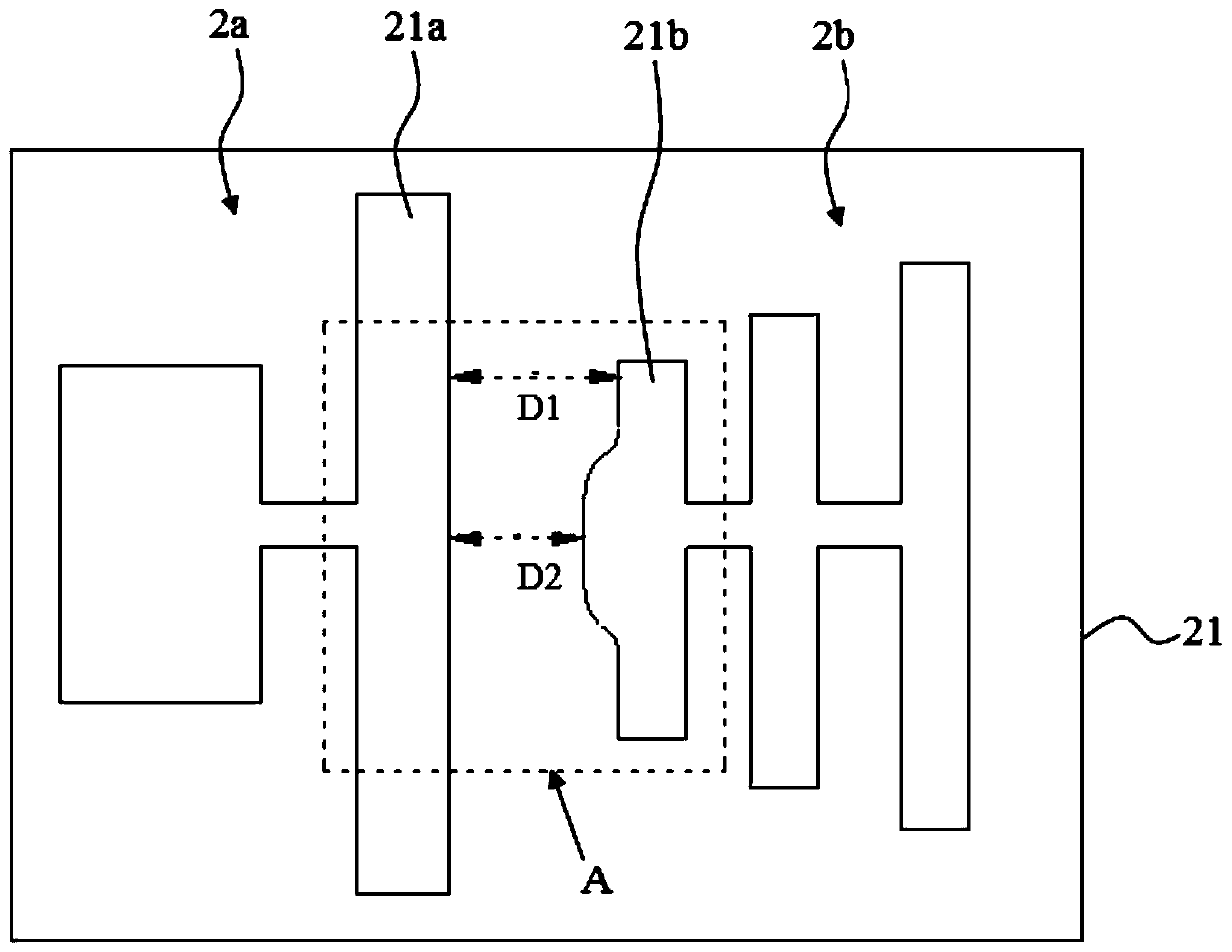
[0025] This embodiment provides an array substrate, figure 1 A schematic diagram of the layout structure of the array substrate is shown, as figure 1 As shown, the ...


PUM

PropertyMeasurementUnit
lengthaaaaaaaaaa

Abstract

The invention discloses an array substrate. The array substrate comprises a display region and a driving circuit region, wherein the driving circuit region is arranged around the display region and comprises a first metal layer, the first metal layer is formed on a substrate, a plurality of metal wires are formed on the first metal layer by a patterning process and comprise a first metal wire anda second metal wire, the first metal wire and the second metal wire are adjacent to each other and are insulated with each other, the distance between the first metal wire and the second metal wire is50 micrometers or above, or the area difference between the first metal wire and the second metal wire does not exceed 10%. The invention also discloses the display device comprising the array substrate.

Description

technical field [0001] The present invention relates to the technical field of displays, in particular to an array substrate, and also to a display device including the array substrate. Background technique [0002] Thin Film Transistor Liquid Crystal Display (TFT-LCD for short) has the characteristics of small size, low power consumption, and no radiation, and occupies a dominant position in the current flat panel display market. GOA (Gate driver On Array) technology is a design in TFT-LCD, which integrates the gate drive circuit of the LCD panel on the substrate to improve the integration of the LCD panel and reduce the usage of the gate drive IC. This is widely used. However, there are some problems in the GOA on the TFT (thin film transistor) substrate in the prior art, wherein it is found that electrostatic discharge (Electrostatic Discharge, ESD) is often defective in the GOA circuit, that is, due to the electrostatic breakdown of the GOA circuit caused by ESD, the TF...

Claims


Application Information

Patent Timeline
Patent Type & Authority Patents(China)
IPC IPC(8): H01L27/12H01L27/02
CPCH01L27/0248H01L27/1214H01L27/124
Inventor 谢剑星杨一峰张骢泷
Owner TCL CHINA STAR OPTOELECTRONICS TECH CO LTD
Why Eureka
Try Eureka