A kind of preparation method of thin film transistor array substrate

A technology of thin film transistors and array substrates, which is applied in the field of preparation of thin film transistor array substrates, and can solve the problems of increased surface resistivity, accelerated surface Cu film oxidation, electrostatic discharge, etc.

Active Publication Date: 2020-10-13
SHENZHEN CHINA STAR OPTOELECTRONICS SEMICON DISPLAY TECH CO LTD
View PDF4 Cites 0 Cited by
  • Summary
  • Abstract
  • Description
  • Claims
  • Application Information

AI Technical Summary

Problems solved by technology

[0003] In the existing array substrate process method, after the deposition of the Cu film, it is exposed to the air through the yellow light process and the etching process, and the Cu on the surface layer will be partially oxidized, and the Cu film is exposed to the air for more than 30 minutes. Its surface resistivity will increase by more than 30%, which will cause the resistivity of Cu line to increase; and the CuO produced on the Cu film x and Cu(OH) x It will lead to Electro-Static discharge (ESD) phenomenon and affect the display effect of TFT devices; the thicker the Cu film, the larger the grain size, the larger the surface roughness, and the larger the gaps in the grain boundaries , so in the follow-up process, there will be some O 2 and H 2 O penetrates into the film along the grain boundary gap, accelerates the oxidation of the surface Cu film, produces electrostatic breakdown or local parasitic capacitance, and further affects the display effect of TFT devices

Method used


Image

  • A kind of preparation method of thin film transistor array substrate
  • A kind of preparation method of thin film transistor array substrate
  • A kind of preparation method of thin film transistor array substrate

Examples


Embodiment Construction

[0062] The following will clearly and completely describe the technical solutions in the embodiments of the present invention with reference to the accompanying drawings in the embodiments of the present invention. Obviously, the described embodiments are only some, not all, embodiments of the present invention. Based on the embodiments of the present invention, all other embodiments obtained by those skilled in the art without creative efforts fall within the protection scope of the present invention.

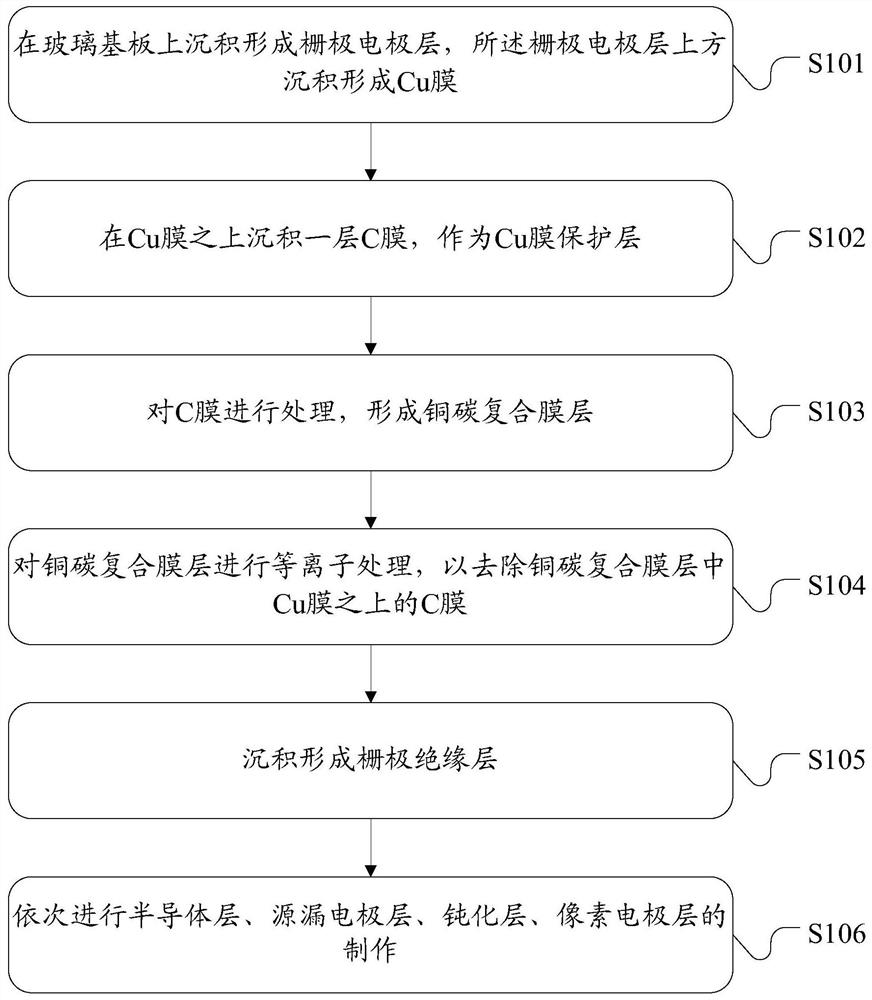
[0063] Thin-film transistor (TFT) is one of the types of field-effect transistors, which are roughly manufactured by depositing various thin films on a substrate, such as semiconductor active layers, dielectric layers, and metal electrode layers. Thin film transistors play a very important role in the performance of display devices.

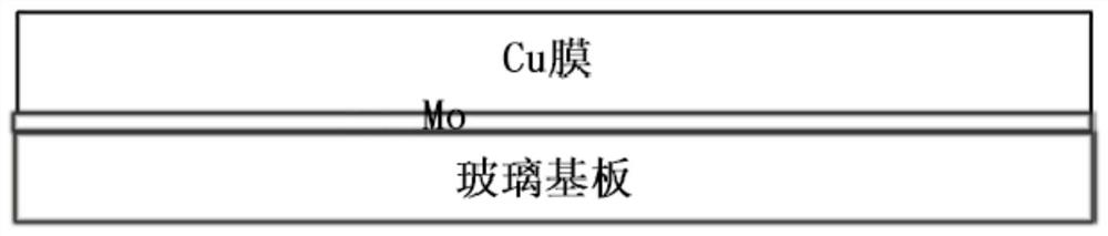
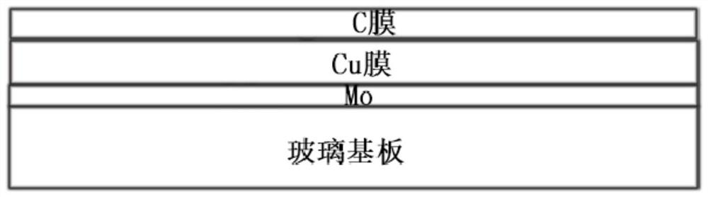
[0064] An embodiment of the present invention provides a method for preparing a thin film transistor array substrate, the method comprising: aft...


PUM

PropertyMeasurementUnit
thicknessaaaaaaaaaa
thicknessaaaaaaaaaa

Abstract

A method for preparing a thin film transistor array substrate. The method comprises the step of: after forming a Cu metal thin film layer on a gate insulating layer and before a yellow light process and an etching process, depositing a C film layer above the Cu metal thin film layer. In the embodiments of the present invention, the Cu film surface electrical resistivity is reduced, preventing the phenomenon of ESD produced by the Cu film and improving the display effects of the thin film transistor array substrate.

Description

technical field [0001] The invention relates to the technical field of semiconductor materials, in particular to a method for preparing a thin film transistor array substrate. Background technique [0002] With the development of flat panel display technology, people's pursuit of display size, resolution and picture refresh rate is getting higher and higher, so copper is used instead of aluminum as the conductive metal material. [0003] In the existing array substrate process method, after the Cu film is deposited, after the yellow light process and the etching process, it is exposed to the air, and the Cu on the surface layer will be partially oxidized, and the Cu film is exposed to the air for more than 30 minutes. Its surface resistivity will increase by more than 30%, which will cause the resistivity of Cu line to increase; and the CuO produced on the Cu film x and Cu(OH) x It will lead to Electro-Static discharge (ESD) phenomenon and affect the display effect of TFT ...

Claims


Application Information

Patent Timeline
Patent Type & Authority Patents(China)
IPC IPC(8): H01L21/28H01L29/423H01L29/49
CPCH01L29/401H01L29/42384H01L29/4908H01L2029/42388
Inventor 胡小波
Owner SHENZHEN CHINA STAR OPTOELECTRONICS SEMICON DISPLAY TECH CO LTD
Why Eureka
Try Eureka