storage device

A storage device and storage array technology, applied in the direction of electrical components, electrical solid-state devices, circuits, etc., can solve the problems of increasing the area occupied by the well voltage extraction area, constrained lithography process limit, and unfavorable utilization of semiconductor substrates. Achieve the effects of reducing the occupied area, reducing production costs and improving utilization

Active Publication Date: 2016-01-20
NAN YA TECH
View PDF3 Cites 0 Cited by
  • Summary
  • Abstract
  • Description
  • Claims
  • Application Information

AI Technical Summary

Problems solved by technology

However, increasing the area occupied by the well voltage extraction region will be detrimental to the utilization of the semiconductor substrate
In addition, in the known technology, the area occupied by the well voltage extraction region can be reduced by reducing the inclination angle of ion implantation, but this method is limited by the process limit of the photolithography process

Method used


Image

  • storage device
  • storage device

Examples


Embodiment Construction

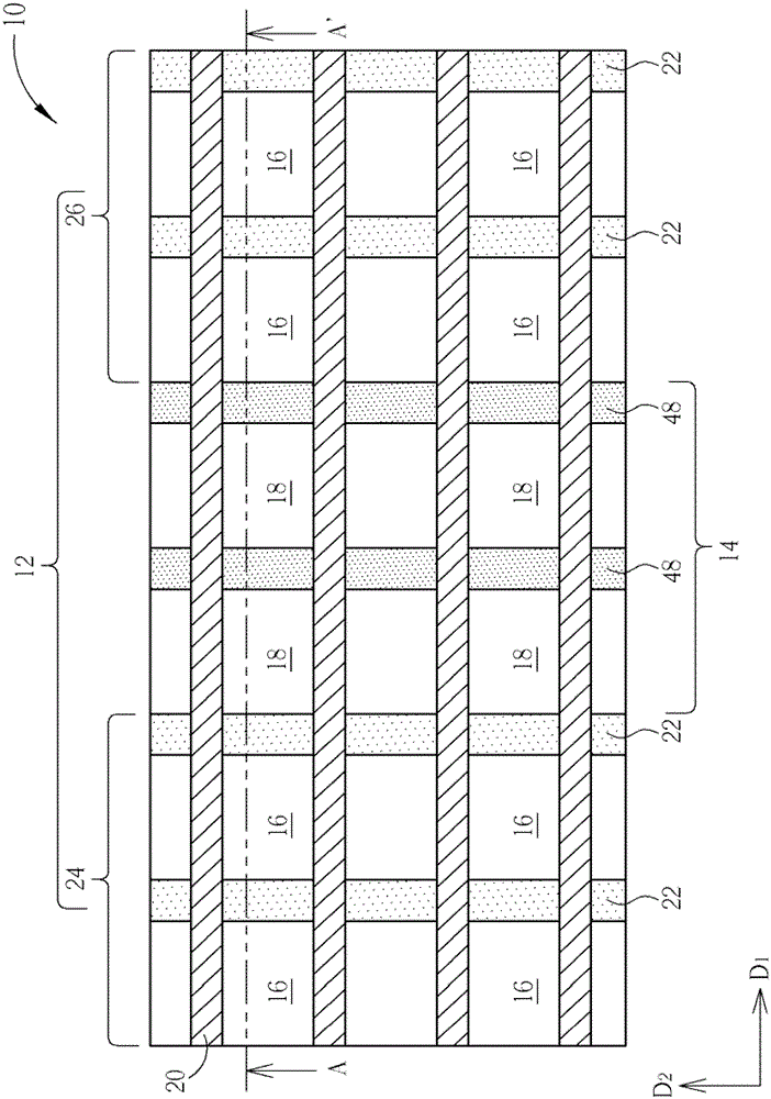
[0026] figure 1 It is a schematic diagram of a storage device according to a preferred embodiment of the present invention. Such as figure 1 As shown, the memory device 10 includes a memory array 12 and at least one well voltage extraction region 14 . The memory array 12 includes a plurality of vertical transistors 16 electrically coupled to corresponding word lines 20 and buried bit lines 22, wherein the word lines 20 extend along a first direction D1, and the buried bit lines 22 extend along a second direction D2. , and the first direction D1 is substantially perpendicular to the second direction D2. The well voltage extraction region 14 includes at least one transistor structure 18 for releasing the well region of the memory device 10 ( figure 1 (not shown) accumulated electrons to adjust the voltage of the well region. In addition, the well voltage extraction region 14 traverses the memory array 12 along the second direction D2, and the memory array 12 is divided into t...


PUM


Abstract

The invention discloses a storage apparatus, comprising a storage array and at least one trap voltage extraction zone. The storage array comprises a plurality of vertical transistors respectively electrically coupling to corresponding word lines and earthed bit lines, wherein the word lines extend along a first direction and the earthed bit lines extend along a second direction. In addition, the trap voltage extraction zone crosses the storage array along the second direction to separate the storage array into a first storage array zone and a secondary storage array zone.

Description

technical field [0001] The present invention relates to a memory device, especially a memory device including a well voltage extraction region. Background technique [0002] In order to increase the operating speed of integrated circuits and at the same time meet consumer demand for miniaturized electronic devices, the size of transistors used in semiconductor devices continues to shrink. When the thickness of the gate oxide layer in Metal-Oxide-Semiconductor (MOS) transistors becomes thinner and thinner, the gate oxide layer is easily damaged by excess charge caused by electrostatic discharge (ESD) phenomenon . As known to those skilled in the art, the electric field strength across the gate oxide is typically greater than 10 7 V / cm, it will cause permanent damage to the gate oxide layer, which will affect the operation of the integrated circuit. [0003] In order to avoid excessive charge accumulation in the semiconductor substrate, the known technology is to arrange th...

Claims


Application Information

Patent Timeline
Patent Type & Authority Patents(China)
IPC IPC(8): H01L27/02H01L27/105
Inventor 陈逸男徐文吉叶绍文刘献文
Owner NAN YA TECH
Why Eureka
Try Eureka