In-situ multifunctional probe testing device for photoelectric device

An optoelectronic device and multifunctional technology, which is applied in the field of in-situ multifunctional optoelectronic device probe testing devices, can solve the problems of lack of test results, complicated operation steps and high cost, and achieve objective and accurate test results and convenient and fast testing process. , the effect of improving test efficiency

Inactive Publication Date: 2014-10-08
NANJING UNIV OF POSTS & TELECOMM
View PDF7 Cites 3 Cited by
  • Summary
  • Abstract
  • Description
  • Claims
  • Application Information

AI Technical Summary

Problems solved by technology

[0006] ① The photoelectric device is exposed to the air during measurement. When the photoelectric device is sensitive to moisture and oxygen, the repeatability of the performance test of the photoelectric device is not good. If it is tested in a glove box or after packaging, the operation steps are complicated and the cost is high;
[0007] ②Because the electrodes of photoelectric devices are generally thin, and the electrodes of photoelectric devices need to be clamped manually with clips during testing, the electrodes are often damaged due to improper manual operation, and accurate test results cannot be obtained;
[0008] ③ During the test, manual operation is required, point by point measurement, complex operation and low efficiency

Method used


Image

  • In-situ multifunctional probe testing device for photoelectric device

Examples


Embodiment Construction

[0016] The specific implementation manners of the present invention will be further described in detail below in conjunction with the accompanying drawings.

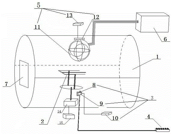
[0017] Such as figure 1 As shown, a kind of in-situ multifunctional photoelectric device probe testing device designed by the present invention includes a sealed test chamber 1, a sample table 2, a probe array device 3, a wiring slot 4, a signal acquisition / transmission device 5, a photoelectric test Instrument 6, the third electronically controlled rotary lifting device 14 and the third controller 15; wherein, the sealed test chamber 1 is provided with a sealed door 7, and the sample table 2 is connected with the third electronically controlled rotary lifted device 14 and arranged in the sealed test chamber Inside the body 1, the third controller 15 is located outside the sealed test chamber 1, and the third controller 15 is connected to the third electronically controlled rotary lifting device 14 through wires; the pro...


PUM


Abstract

The invention relates to an in-situ multifunctional probe testing device for a photoelectric device. A brand new testing device is designed, based on the device, the photoelectric device can be tested automatically under various different environments of vacuum, nitrogen, oxygen and the like, by the aid of a probe touch mode, automatic operation can be achieved in a sealing test cavity in the whole process, the photoelectric device can be protected, the testing process is convenient and swift, the testing result is objective and accurate, and the testing efficiency of the photoelectric device is greatly improved.

Description

technical field [0001] The invention relates to an in-situ multifunctional photoelectric device probe testing device. Background technique [0002] At present, a variety of optoelectronic devices are widely used in people's daily life, and the research and development of each optoelectronic device requires repeated testing of its performance, so as to optimize its structure and evaluate its performance stability. The traditional test method in the laboratory is to place the photoelectric device in a glove box or in the air and measure it point by point manually. Taking the test of organic light-emitting diode (OLED) as an example, three sets of parameters are generally measured: the current-voltage curve of the light-emitting point, the brightness and spectrum. The test methods of organic light-emitting diodes in the laboratory include the following: [0003] Clamp the positive and negative poles of a light-emitting point of the organic light-emitting diode device with a c...

Claims


Application Information

Patent Timeline
Patent Type & Authority Applications(China)
IPC IPC(8): G01R31/26G01R1/073H02S50/10
CPCY02E10/50
Inventor 陈润锋宋超林诚黄维
Owner NANJING UNIV OF POSTS & TELECOMM
Why Eureka
Try Eureka