Method for optimizing exposure auxiliary graph

A technology for assisting graphics and optimization methods, applied to the photographic process of patterned surfaces, originals for photomechanical processing, optics, etc.

Active Publication Date: 2014-10-08
SHANGHAI HUALI MICROELECTRONICS CORP
View PDF6 Cites 17 Cited by
  • Summary
  • Abstract
  • Description
  • Claims
  • Application Information

AI Technical Summary

Problems solved by technology

[0011] In order to achieve the purpose of the present invention, the present invention provides an optimization method for exposure auxiliary graphics to solve (especially in the case of small nodes and complex graphics) the optimization problem of adding rules for exposure auxiliary graphics

Method used


Image

  • Method for optimizing exposure auxiliary graph
  • Method for optimizing exposure auxiliary graph
  • Method for optimizing exposure auxiliary graph

Examples


Embodiment Construction

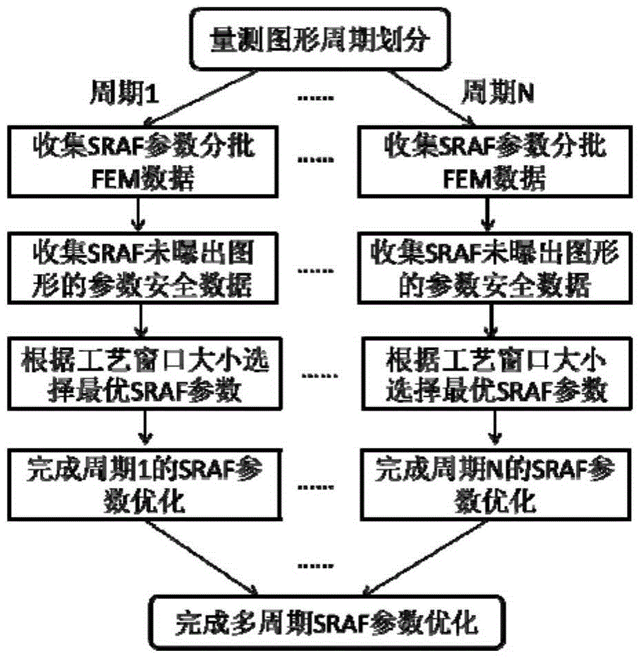
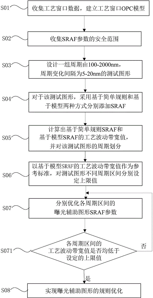
[0033] see figure 2 , the optimization method of the exposure assistance figure of the present embodiment comprises the following steps:

[0034] Step S01, collect OPC test pattern data of multiple energy and focal depth conditions within the process window, and establish an OPC model of the process window.

[0035] Step S02 , collecting a safe range of SRAF parameters, where the safe range of parameters is a safe range of parameters of the SRAF in which no pattern is exposed within the process window. For example, when the width of the exposure auxiliary patterns is 20-45nm, the distance between the exposure auxiliary patterns and the main pattern is 50-100nm, and the distance between the exposure auxiliary patterns is 50-100nm.

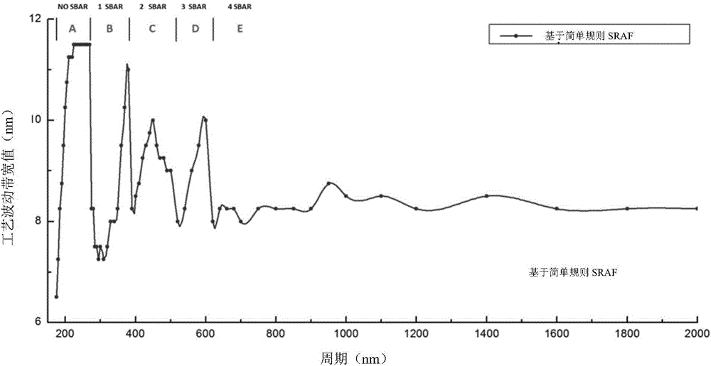
[0036] Step S03 , designing a group of 1D line or 2D hole test patterns with a period of 100-2000nm and a period change interval of 5-20nm according to the pattern characteristics of the lithography layer.

[0037] In step S04, for the test patte...


PUM


Abstract

The invention discloses a method for optimizing an exposure auxiliary graph. The method comprises the following steps: collecting process window data and establishing an OPC (Optical Proximity Correction) model of a process window; collecting a safe range of SRAF (Sub Resolution Assist Feature) parameters; designing a periodic gradient test graph; adding SRAF based on simple rules and the model; obtaining a process fluctuation bandwidth value and dividing the test graph into periods; setting process fluctuation bandwidth upper limit values for period zones of the test graph; respectively optimizing the SRAF parameters of the exposure auxiliary graph of the period zones; and optimizing the rules of the exposure auxiliary graph. The method for optimizing the exposure auxiliary graph is capable of efficiently and quickly optimizing the addition rules of the exposure auxiliary graph and reducing the operation quantity; compared with that by adopting a method based on the model, the operation time can be reduced by about 60%.

Description

technical field [0001] The invention relates to the technical field of semiconductor manufacturing, in particular to an optimization method of an exposure auxiliary pattern. Background technique [0002] The rapid development of the semiconductor industry is mainly due to the progress of micro-processing technology in microelectronics technology, and photolithography technology is one of the most critical manufacturing technologies in chip preparation. Due to the continuous innovation of optical lithography technology, it has repeatedly broken through the expected optical exposure limit, making it the mainstream technology of current exposure. [0003] The lithography system mainly includes four parts: illumination system (light source), mask, projection system and wafer. The light incident on the mask is diffracted, and the diffracted light enters the projection system and forms an interference image on the wafer. After developing and etching, the pattern is transferred to...

Claims


Application Information

Patent Timeline
Patent Type & Authority Applications(China)
IPC IPC(8): G03F1/36
Inventor 张月雨毛智彪张瑜
Owner SHANGHAI HUALI MICROELECTRONICS CORP
Why Eureka
Try Eureka