Embedded-type touch screen and display device

A built-in touch screen, integrated technology, applied in optics, instruments, electrical and digital data processing and other directions, can solve the problems of touch screen touch failure, affecting touch screen display, etc., to prevent interference and damage.

Inactive Publication Date: 2014-10-08
BOE TECH GRP CO LTD +1
View PDF5 Cites 41 Cited by
  • Summary
  • Abstract
  • Description
  • Claims
  • Application Information

AI Technical Summary

Problems solved by technology

However, due to the good conductivity of ITO material, it will shield the touch signal, which will cause the touch function of the touch screen to fail and seriously affect the touch display of the touch screen.

Method used


Image

  • Embedded-type touch screen and display device
  • Embedded-type touch screen and display device
  • Embedded-type touch screen and display device

Examples


Embodiment 1

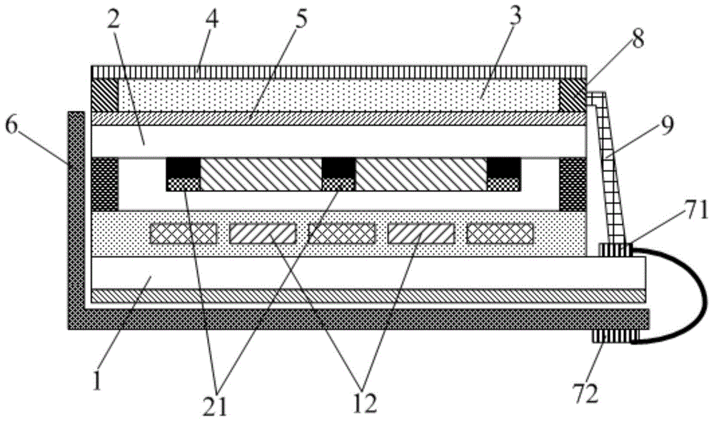
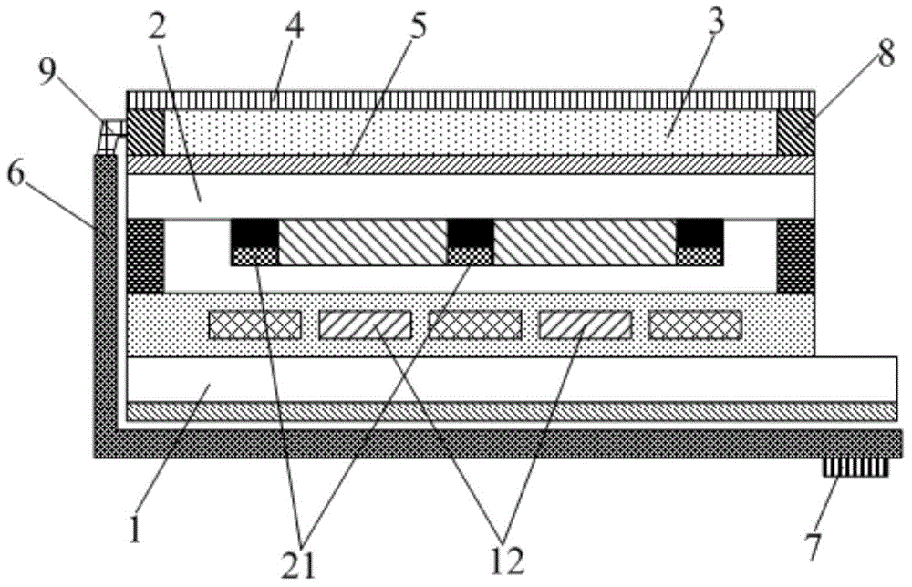
[0034] This embodiment provides an embedded touch screen, such as figure 1 As shown, it includes an array substrate 1 and a color filter substrate 2 that are arranged oppositely, and the touch electrodes (that is, the driving electrodes 12 and the sensing electrodes 21) are arranged between the array substrate 1 and the color filter substrate 2. 2, the electrostatic release layer 3 on the side away from the array substrate 1, the electrostatic release layer 3 is a transparent conductive layer with a sheet resistance above the megohm level.

[0035] Wherein, the sheet resistance of the electrostatic discharge layer 3 ranges from greater than or equal to 1MΩ to less than or equal to 1kMΩ. The electrostatic release layer 3 with the resistance value of the square resistance can discharge the static electricity well, and will not shield the touch signal of the touch screen, so that the touch screen can well prevent the interference or destruction of static electricity, and can Tou...

Embodiment 2

[0047] This embodiment provides an embedded touch screen. The difference from Embodiment 1 is that the electrostatic discharge layer of the touch screen does not use insulating optical adhesive materials doped with conductive particles, but uses other materials that meet the requirements of the square resistance value of megohms. Transparent conductive materials above the level, for example: transparent conductive materials formed by doping PEDOT (polyethylenedioxythiophene) particles in insulating resin materials, or transparent conductive materials formed by doping indium antimony oxide particles in SiO2 insulating materials etc., these transparent conductive materials can be formed on the substrate by coating. Among them, the PEDOT particles or the indium antimony oxide particles are also connected by molecular formula or chemical bond, so that the static electricity accumulated on the static electricity release layer 3 can be conducted away.

[0048] In this example, if ...

Embodiment 3

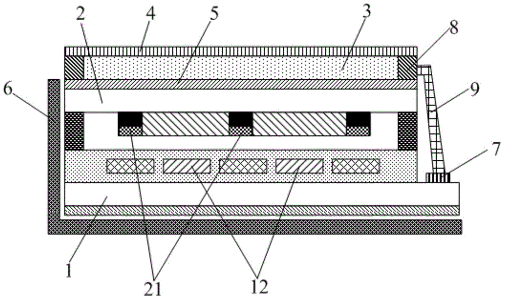
[0051] This embodiment provides an embedded touch screen, and the difference from Embodiment 1-2 is that, as Figure 5 As shown, the touch screen also includes an adhesive layer 10, the upper polarizer 5, the adhesive layer 10 and the electrostatic release layer 3 are sequentially laminated on the color filter substrate 2, the cover plate 4 is covered on the electrostatic release layer 3, and the adhesive The layer 10 can bond the cover plate 4 and the color filter substrate 2 together. Wherein, the electrostatic discharge layer 3 is directly coated on the top of the cover plate 4, and the adhesive layer 10 is a non-conductive layer having an adhesive effect.

[0052] In addition, in this embodiment, the first ground terminal 71 is connected to the electrostatic discharge layer 3 through the conductive silver paste 9 and the conductive tape 11, and the conductive tape 11 is arranged on the edge area of ​​the in-cell touch screen corresponding to the non-touch display area. In...


PUM


Abstract

The invention provides an embedded-type touch screen and a display device. The embedded-type touch screen comprises an array substrate, a color film substrate and an electrostatic discharge layer, wherein the array substrate and the color film substrate are folded in an alignment mode; a touch electrode is arranged between the array substrate and the color film substrate; the electrostatic discharge layer is arranged on one side, far away from the array substrate, of the color film substrate; the electrostatic discharge layer is a transparent conductive layer of which the resistance value of a square resistor is greater than a mega-ohm level. By the arrangement of the transparent electrostatic discharge layer of which the resistance value of the square resistor is greater than the mega-ohm level, the embedded-type touch screen can well discharge static electricity, and a touch signal of the touch screen cannot be shielded, so that the touch screen can be used for well preventing electrostatic interference and damage, and can be normally touched for display.

Description

technical field [0001] The present invention relates to the field of display technology, in particular to an embedded touch screen and a display device. Background technique [0002] Since an in-cell touch panel (in cell touch panel) can make the screen thinner and lighter, the in-cell touch panel is more and more widely used in the display panel at present. [0003] For example: currently a common ADS (Advanced Super Dimensional Field Switching Display Mode) embedded touch screen, usually the touch drive electrodes (TX) and touch sensing electrodes (RX) are designed on the combination of the array substrate and the color filter substrate The inside of the formed liquid crystal cell is specifically as follows: the common electrode layer arranged on the array substrate is divided into two parts, one part is used as a common electrode, and the other part is multiplexed as a touch driving electrode (TX) during touch control, and a touch sensing electrode (TX). RX) is arranged ...

Claims


Application Information

Patent Timeline
Patent Type & Authority Applications(China)
IPC IPC(8): G06F3/041
CPCH01L23/60G02F1/13338G02F1/136204G06F3/0412G02F1/133514G02F1/133528G06F2203/04107
Inventor 刘英明董学王海生丁小梁杨盛际
Owner BOE TECH GRP CO LTD
Why Eureka
Try Eureka