Switch control band-gap reference circuit with low offset voltage

A technology of offset voltage and switch control, which is applied in the direction of control/adjustment system, adjustment of electrical variables, instruments, etc., can solve the problem of reducing the accuracy of the reference voltage signal, and achieve the effect of improving accuracy and reducing input offset voltage

Inactive Publication Date: 2014-10-22
SHENZHEN KECHUANGDA MICRO ELECTRONICS CO LTD
View PDF9 Cites 0 Cited by
  • Summary
  • Abstract
  • Description
  • Claims
  • Application Information

AI Technical Summary

Problems solved by technology

[0004] This traditional bandgap reference circuit has an input offset voltage that degrades the accuracy of the reference voltage signal

Method used


Image

  • Switch control band-gap reference circuit with low offset voltage
  • Switch control band-gap reference circuit with low offset voltage
  • Switch control band-gap reference circuit with low offset voltage

Examples


Embodiment 1

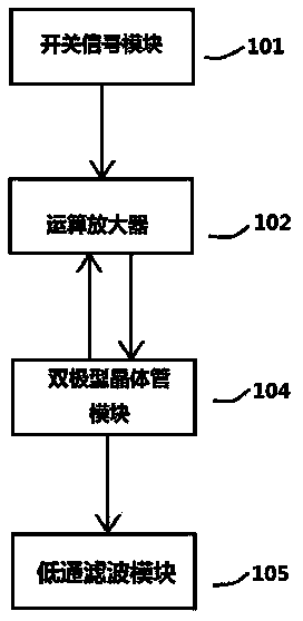
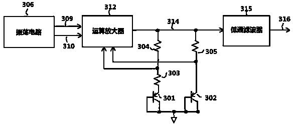
[0025] Such as figure 1 As shown, a switch-controlled bandgap reference circuit with low offset voltage includes a switch signal module 101, an operational amplifier 102, a bipolar transistor module 104 and a low-pass filter module 105, and the output terminal of the switch signal module 101 is connected to the The input terminal of the operational amplifier 102 is connected, the output terminal of the operational amplifier 102 is connected with the bipolar transistor module 104, and the bipolar transistor module 104 is connected with the low-pass filter module 105; the switch signal Module 101 includes a first switch signal output terminal and a second switch signal output terminal, the first switch signal output terminal is connected to the non-inverting input terminal of the operational amplifier 102, and the second switch signal output terminal is connected to the operational amplifier 102 is connected to the inverting input terminal, one end of the bipolar transistor mod...

Embodiment 2

[0033] Embodiment two is based on embodiment one.

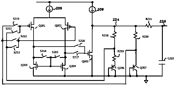
[0034] Such as figure 2 As shown, the operational amplifiers 102 and 312 are preferably two-stage operational amplifiers.

[0035] Such as figure 2 As shown, the operational amplifiers 102 and 312 include PMOS transistors Q201, PMOS transistors Q202, NMOS transistors Q203, NMOS transistors Q204, and NMOS transistors Q205, and the switch signal module 101 includes switches S210, S211, S212, S213, S214, and S215 , S216, the first bipolar transistor 302 is a PNP transistor Q206, the second bipolar transistor 301 is a PNP transistor Q207, the first resistor 305 is a resistor R220, and the second resistor 304 is a resistor R218 , the third resistor 303 is a resistor R219, wherein the emitter of the PNP transistor Q207 is respectively connected to one end of the switches S210 and S212, the other end of the switch S210 is connected to the gate of the PMOS transistor Q201, and the gate of the switch S212 The other end is connect...


PUM

PropertyMeasurementUnit
Temperature coefficientaaaaaaaaaa

Abstract

The invention provides a switch control band-gap reference circuit with the low offset voltage. The switch control band-gap reference circuit comprises a switching signal module, an operational amplifier, a bipolar transistor module and a low-pass filtering module. The output end of the witching signal module is connected with the input end of the operational amplifier, the output end of the operational amplifier is connected with the bipolar transistor module, and the bipolar transistor module is connected with the low-pass filtering module. The switching signal module comprises a first switching signal output end and a second switching signal output end, the first switching signal output end is connected with the in-phase input end of the operational amplifier, and the second switching signal output end is connected with the inverted input end of the operational amplifier. The switch control band-gap reference circuit has the advantages that the input offset voltage of the operational amplifier is lowered, and the accuracy of band-gap reference voltage signals is improved.

Description

technical field [0001] The invention relates to a bandgap reference circuit, in particular to a bandgap reference circuit with low offset voltage controlled by a switch. Background technique [0002] In recent years, with the rapid development of the electronic industry and the field of integrated circuits, the performance of integrated circuits required by the system has gradually improved. For the bandgap reference circuit used in the circuit, the requirements for the accuracy of its reference voltage are also getting higher and higher. The existing bandgap The accuracy of the reference voltage of the gap reference circuit is low, and it has become increasingly difficult to meet the requirements of use. [0003] Such as Figure 4 As shown, the traditional bandgap reference circuit diagram includes an operational amplifier 401, a PNP transistor 405 and a PNP transistor 406, the emitter of the PNP transistor 406 is connected to the VP terminal of the operational amplifier 40...

Claims


Application Information

Patent Timeline
IPC IPC(8): G05F1/56
Inventor 张君志贾相英
Owner SHENZHEN KECHUANGDA MICRO ELECTRONICS CO LTD
Why Eureka
Try Eureka