

Finned bipolar junction transistor and manufacturing method thereof
A bipolar junction and transistor technology, applied in the manufacture of transistors, semiconductor devices, semiconductor/solid-state devices, etc., can solve the problems of PN junction position variation and small PN junction area of fin bipolar junction transistors
- Summary
- Abstract
- Description
- Claims
- Application Information
AI Technical Summary
Problems solved by technology
Method used
Image

Examples
no. 1 Embodiment
[0053] This embodiment will describe in detail the method of fabricating a fin bipolar junction transistor.
[0054] Figure 4A to Figure 6B It is a structural schematic diagram of the method for preparing a fin bipolar junction transistor in this specific embodiment, which will be combined below Figure 4A to Figure 6B A first embodiment of the present invention will be described in detail.
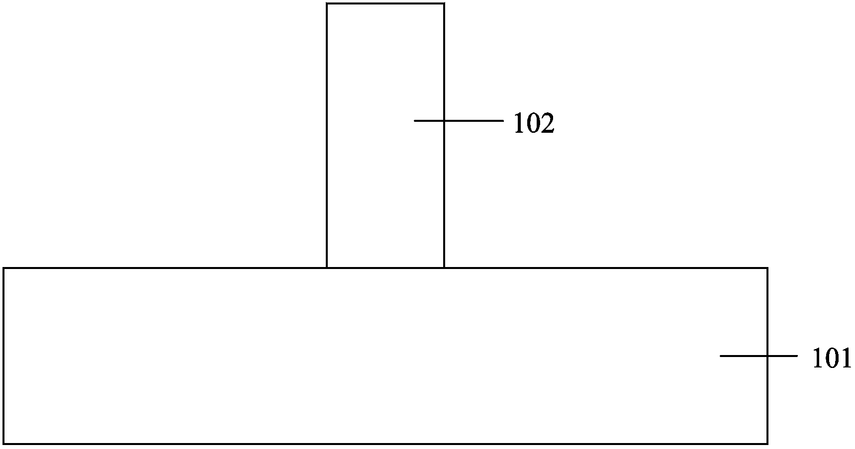
[0055] first reference Figures 4A-4C , providing a substrate 201; forming a fin portion 202 doped with impurities on the substrate 201 as a base region, and the fin portion 202 includes a first region 2021 and a second region 2023 separated from each other.
[0056] Figure 4A is a schematic diagram of a three-dimensional structure of a fin 202 doped with impurities formed on a substrate 201, Figure 4B for Figure 4A The sectional view of the plane cut by the median line A-A', Figure 4C for Figure 4A Sectional view of the plane cut by the median line B-B'.
[0057] In a speci...
no. 2 Embodiment
[0076] This embodiment is an embodiment of a fin bipolar junction transistor.
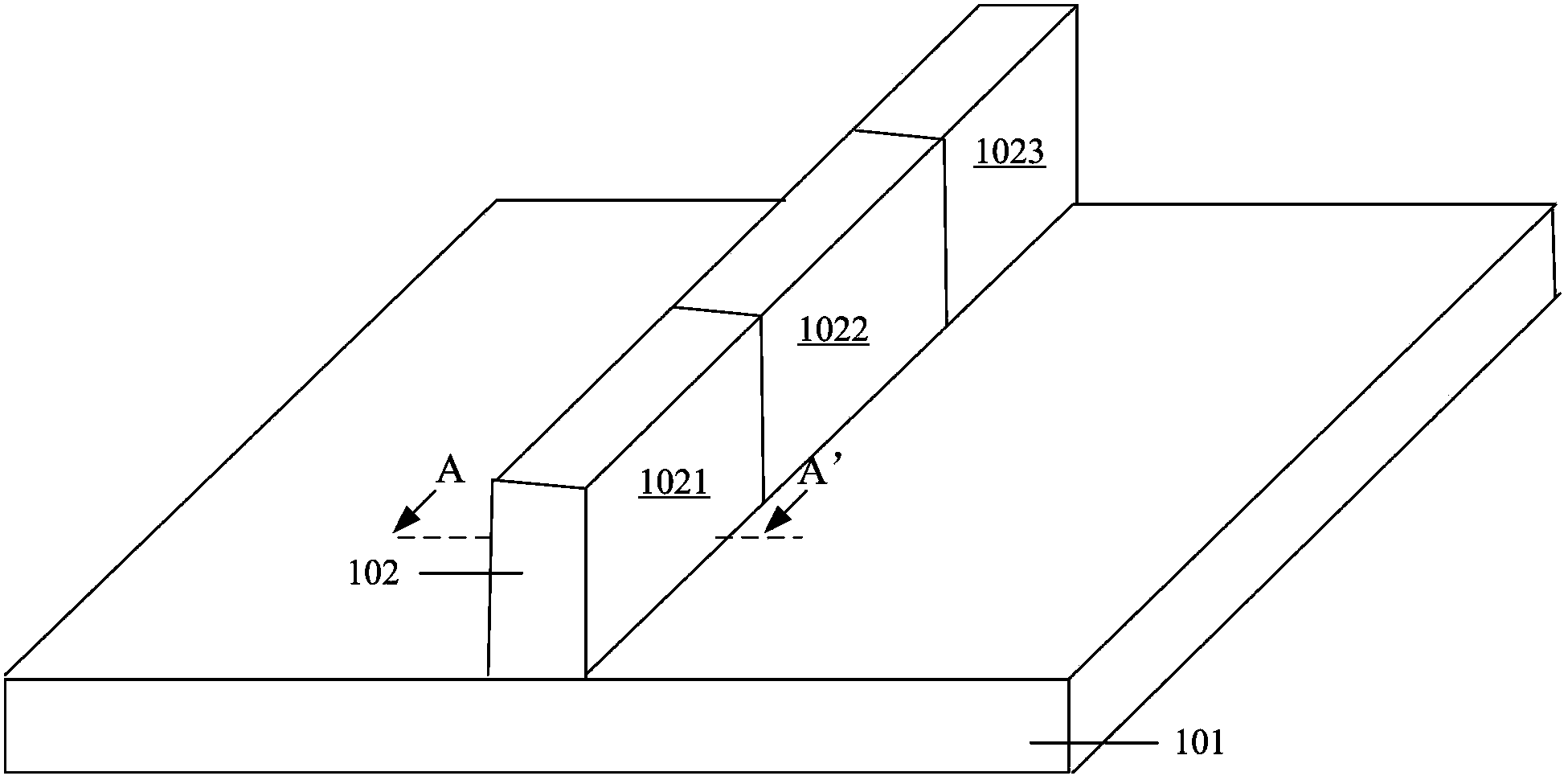
[0077] refer to Figures 5A-6B , the fin bipolar junction transistor includes: a substrate 201; a fin 202 located on the substrate 201, the fin 202 is a base region; the fin 202 includes a first region 2021 and a second region separated from each other A region 2023; a collector region located on the first region 2021; an emission region located on the second region 2023.
[0078] refer to Figure 6A and 6B , the fin portion 202 further includes a third region 2022 located between the first region 2021 and the second region 2023 .
[0079] In a specific embodiment, the material of the substrate 201 may be silicon, silicon germanium, silicon-on-insulator, and in other embodiments, it may also be other conventional semiconductor materials well known in the art.
[0080] In a specific embodiment, the fin bipolar junction transistor is a PNP transistor, the material of the fin portion 202 is SiC, a...
no. 3 Embodiment
[0084] This embodiment will describe in detail the method of fabricating a fin bipolar junction transistor.
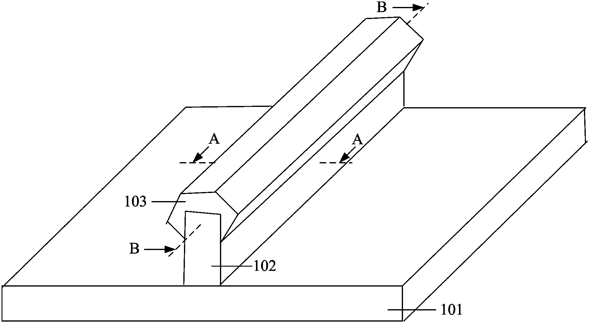
[0085] Figure 7A to Figure 8B It is the structure schematic diagram of the preparation fin bipolar junction transistor of this specific embodiment, will combine below Figure 7A to Figure 8B , the technical solution of the present invention will be described in detail.
[0086] first reference Figures 7A-7C , providing a substrate 301; forming a fin 302 doped with impurities on the substrate 301 as an emission region, and the fin 302 includes a first region 3021 and a second region 3022 in contact with each other.
[0087] In a specific embodiment, the total length of the first region 3021 and the second region 3022 is smaller than the length of the fin 302, so as to reserve a space on the fin 302 and form a contact electrode on the fin 302; if There is no need to reserve space for the formation of contact electrodes, and the total length of the first region 3021 ...
PUM
 Abstract
Description
Claims
Application Information