Bias circuit

a bias circuit and bias circuit technology, applied in the direction of electric variable regulation, process and machine control, instruments, etc., can solve the problems of unstable negative feedback in the bias circuit, insufficient amount of feedback of the bias circuit, and difficulty in obtaining high voltage gain, so as to improve the signal amplification linearity

Active Publication Date: 2021-01-14
MURATA MFG CO LTD
View PDF0 Cites 0 Cited by
  • Summary
  • Abstract
  • Description
  • Claims
  • Application Information

AI Technical Summary

Benefits of technology

[0008]The present disclosure can provide the bias circuit that enables an improvement in sig

Problems solved by technology

However, when the gain band of the bias circuit is widened, a sufficient phase margin is not able to be obtained, and negative feedback in the bias circuit can become unstable.
On the other hand, when the bias circuit is used in

Method used


Image

  • Bias circuit
  • Bias circuit
  • Bias circuit

Examples


first embodiment

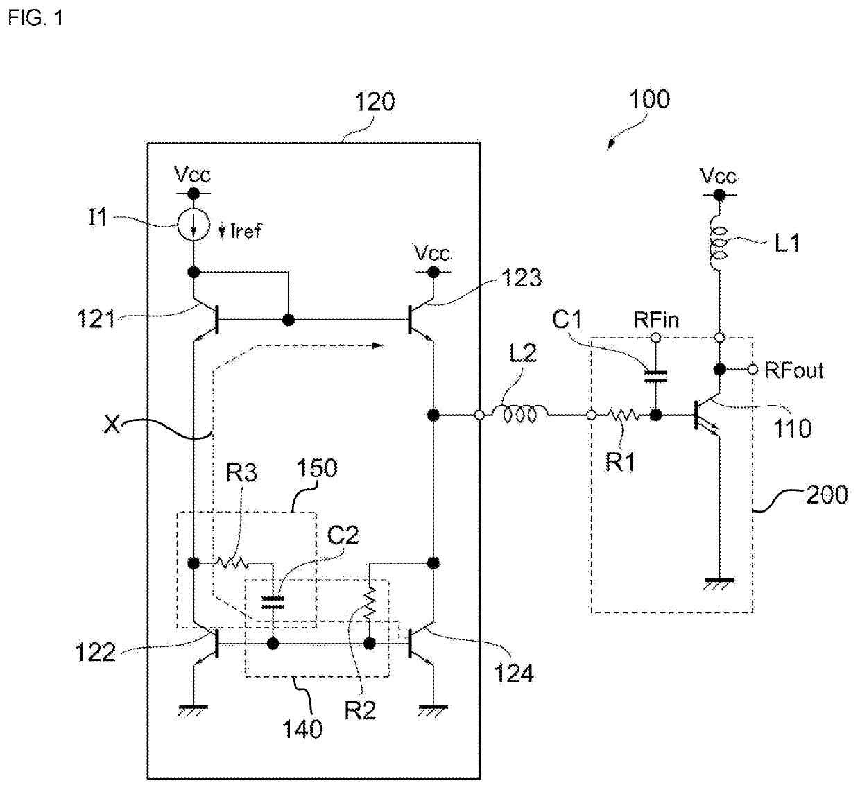
[0018]FIG. 1 illustrates an example of a configuration of a power amplifier circuit including a bias circuit according to the present disclosure. A power amplifier circuit 100 is installed, for example, in a mobile communication device, such as a cellular phone, and is used to amplify power of a radio frequency (RF) signal to be transmitted to a base station. The power amplifier circuit 100 amplifies transmission signals of communication standards, such as the second generation mobile communication system (2G), the third generation mobile communication system (3G), the fourth generation mobile communication system (4G), the fifth generation mobile communication system (5G), long term evolution (LTE)-frequency division duplex (FDD), LTE-time division duplex (TDD), LTE-Advanced, and LTE-Advanced Pro. A fundamental band of an RF signal ranges, for example, from about several hundred MHz to about several tens of GHz. A communication standard and a fundamental band of a signal to be ampl...

third embodiment

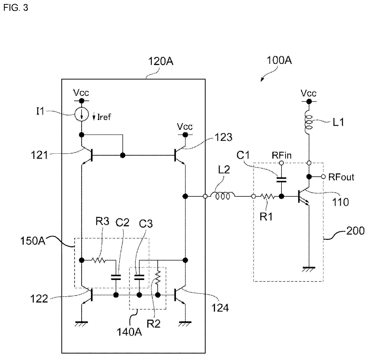
[0055]FIG. 4 illustrates an example of a configuration of a power amplifier circuit including a bias circuit according to the present disclosure. As illustrated in FIG. 4, a power amplifier circuit 100B includes a bias circuit 120B in place of the bias circuit 120 in comparison with the above-described power amplifier circuit 100. The bias circuit 120B includes an inductor L3 in place of the resistance element R3 in comparison with the bias circuit 120.

[0056]The inductor L3 is connected in series with the capacitor C2 between the collector and base of the transistor 122. The inductor L3 and the capacitor C2 constitute a high pass filter circuit 150B.

[0057]Thus, a combination of elements constituting a high pass filter circuit is not limited to a combination of a resistance element and a capacitor and may be a combination of other elements, such as an inductor and so forth.

[0058]FIGS. 5 to 7 respectively illustrate power amplifier circuits 100C to 100E corresponding to modifications ...


PUM


Abstract

A bias circuit includes first to fourth transistors and a phase compensation circuit. In the first transistor, a reference current or voltage is supplied to a first terminal, and the first terminal and a second terminal are connected. In the second transistor, a first terminal is connected to the first transistor, and a third terminal is grounded. In the third transistor, a power supply voltage is supplied to a first terminal, a second terminal is connected to the first transistor, and a bias current or voltage is supplied from a third terminal to an amplifier transistor. In the fourth transistor, a first terminal is connected to the third transistor, a second terminal is connected to the second transistor, and a third terminal is grounded. The phase compensation circuit is provided in a path extending from the fourth transistor to the third transistor through the second and first transistors.

Description

[0001]This application claims priority from Japanese Patent Application No. 2019-128866 filed on Jul. 11, 2019. The content of this application is incorporated herein by reference in its entirety.BACKGROUND[0002]The present disclosure relates to a bias circuit. In mobile communication terminals, such as cellular phones, a power amplifier circuit is used that amplifies a radio frequency (RF) signal to be transmitted to a base station. The power amplifier circuit includes, for example, a transistor that amplifies an input signal, and a bias circuit that determines an operating point of the transistor.[0003]In the power amplifier circuit, power gain has to be kept as constant as possible regardless of output power of an RF signal to maintain linearity. For example, Japanese Unexamined Patent Application Publication No. 2018-98766 discloses a power amplifier circuit in which a bias circuit includes a negative feedback path and can inhibit deterioration of linearity by supplying a stable...

Claims


Application Information

Patent Timeline
IPC IPC(8): H03F1/32H03F3/21H03H7/06
CPCH03F1/32H03F2200/451H03H7/06H03F3/21G05F1/567H03H11/04H03H7/0115H03F3/245H03F1/301H03F1/302H03F2200/363H03F2200/18H03F1/3205H03F3/19
Inventor SOGA, TAKASHI
Owner MURATA MFG CO LTD
Why Eureka
Try Eureka