Removable indicator structure in electronic chips of a common substrate for process adjustment

A technology of electronic chips and indicators, applied in the direction of electric solid devices, circuits, electrical components, etc., to achieve the effect of low power consumption and small resistance

Active Publication Date: 2014-11-05
INFINEON TECH AG
View PDF4 Cites 5 Cited by
  • Summary
  • Abstract
  • Description
  • Claims
  • Application Information

AI Technical Summary

Problems solved by technology

[0003] However, there is still potential room for reducing manufacturing costs and simplifying the processing of electronic chips to be packaged while maintaining high processing accuracy

Method used


Image

  • Removable indicator structure in electronic chips of a common substrate for process adjustment
  • Removable indicator structure in electronic chips of a common substrate for process adjustment
  • Removable indicator structure in electronic chips of a common substrate for process adjustment

Examples


Embodiment Construction

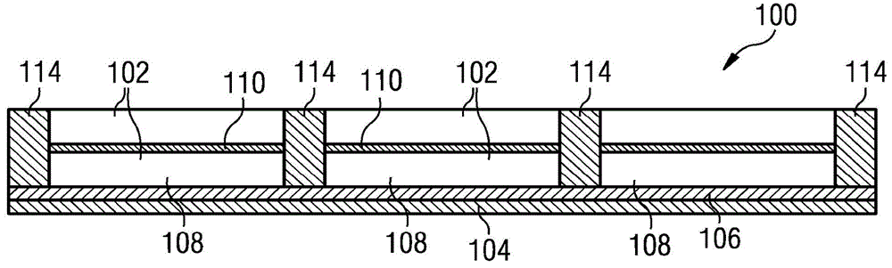
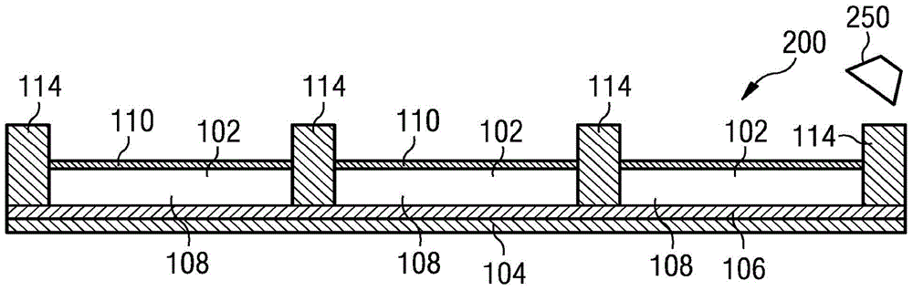
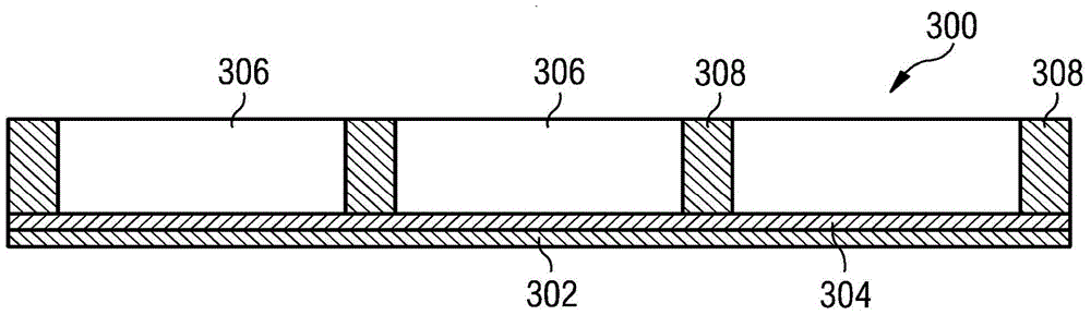
[0057] The illustrations in the figures are schematic.

[0058] A conventional method of etching electronic chips is a timed plasma etch process, where the plasma etch process is terminated when a target depth is reached. The process duration can be calculated using the known etch rate for the semiconductor substrate. However, variations in substrate etch rate (intra-wafer and / or from wafer-to-wafer) translate directly into variations in etch depth, and thus into thinned chips, making it impossible to have a true endpoint.

[0059] In another conventional approach, an etch stop layer is implemented in the semiconductor chip at a target depth to provide an etch stop after exposure of the etch stop layer due to the high selectivity of the etch process to the substrate above the stop layer, That is due to the high ratio of the etch rate of the substrate to the etch rate of the stop layer. However, this approach requires that an etch stop layer must be provided in the semiconduc...


PUM


Abstract

A method of processing a plurality of packaged electronic chips being connected to one another in a common substrate is provided, wherein the method comprises etching the electronic chips, detecting information indicative of an at least partial removal of an indicator structure following an exposure of the indicator structure embedded within at least a part of the electronic chips and being exposed after the etching has removed chip material above the indicator structure, and adjusting the processing upon detecting the information indicative of the at least partial removal of the indicator structure.

Description

technical field [0001] The present invention relates to methods and apparatus for processing a plurality of electronic chips on a substrate level, electronic chips and articles of manufacture. Background technique [0002] Conventional packaging for electronic chips, such as molded structures, has evolved to a level where the packaging no longer significantly hinders the performance of the electronic chips. Furthermore, processing electronic chips on a wafer level is a known process for the efficient production of electronic chips. Etching electronic chips is a conventional technique for removing material from electronic chips. [0003] However, there is still potential to reduce manufacturing costs and simplify the handling of electronic chips to be packaged while maintaining a high accuracy rate of handling. Contents of the invention [0004] It may be desirable to provide the possibility to manufacture electronic chips with a simple processing architecture and with hi...

Claims


Application Information

Patent Timeline
Patent Type & Authority Applications(China)
IPC IPC(8): H01L21/02H01L21/66H01L21/67H01L27/04
CPCH01L21/67253H01L22/24H01L21/67069H01L21/6835H01L21/6836H01L22/26H01L22/30H01L24/19H01L24/96H01L24/97H01L2924/1461H01L2924/18162H01L21/568H01L22/12H01L2224/0401H01L2224/04105H01L2221/6834H01L2221/68327H01L2224/12105H01L2224/94H01L2924/13091H01L2924/13055H01L2924/1306H01L2924/1305H01L2924/181H01L2224/82H01L2924/00H01L21/784
Inventor E·富尔古特I·埃舍尔-珀佩尔M·恩格尔哈特H-J·蒂默H·埃德
Owner INFINEON TECH AG
Why Eureka
Try Eureka