Semiconductor device with multi-layer epitaxial super junction framework, and manufacturing method of semiconductor device

A manufacturing method and super junction technology, applied in semiconductor/solid-state device manufacturing, semiconductor devices, electrical components, etc., can solve the problems of high manufacturing cost, poor reverse recovery characteristics, and long production cycle

Active Publication Date: 2014-11-05
WUXI CHINA RESOURCES MICROELECTRONICS
View PDF3 Cites 4 Cited by
  • Summary
  • Abstract
  • Description
  • Claims
  • Application Information

AI Technical Summary

Problems solved by technology

[0004] Based on this, in order to solve the problems of poor reverse recovery characteristics, high manufacturing cost and long production cycle of the tradition

Method used


Image

  • Semiconductor device with multi-layer epitaxial super junction framework, and manufacturing method of semiconductor device
  • Semiconductor device with multi-layer epitaxial super junction framework, and manufacturing method of semiconductor device
  • Semiconductor device with multi-layer epitaxial super junction framework, and manufacturing method of semiconductor device

Examples


Embodiment Construction

[0017] In order to make the objects, features and advantages of the present invention more comprehensible, specific implementations of the present invention will be described in detail below in conjunction with the accompanying drawings.

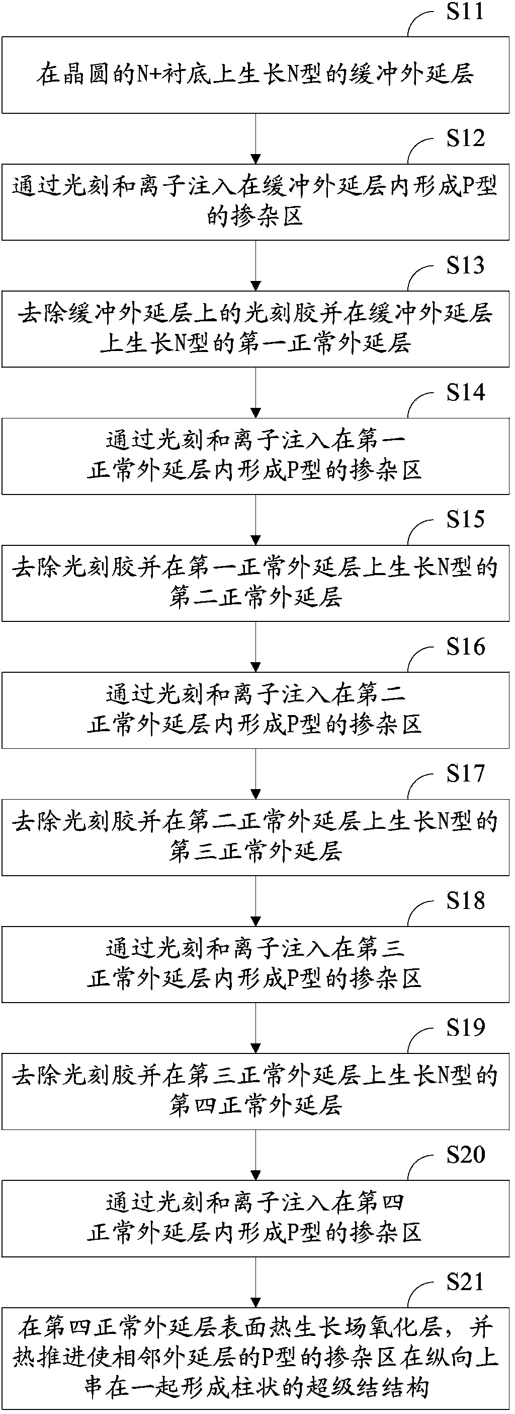
[0018] figure 1 It is a flowchart of a method for manufacturing a semiconductor device with a multilayer epitaxial super junction structure in an embodiment, including the following steps:

[0019] S11, growing an N-type buffer epitaxial layer on the N+ substrate of the wafer.

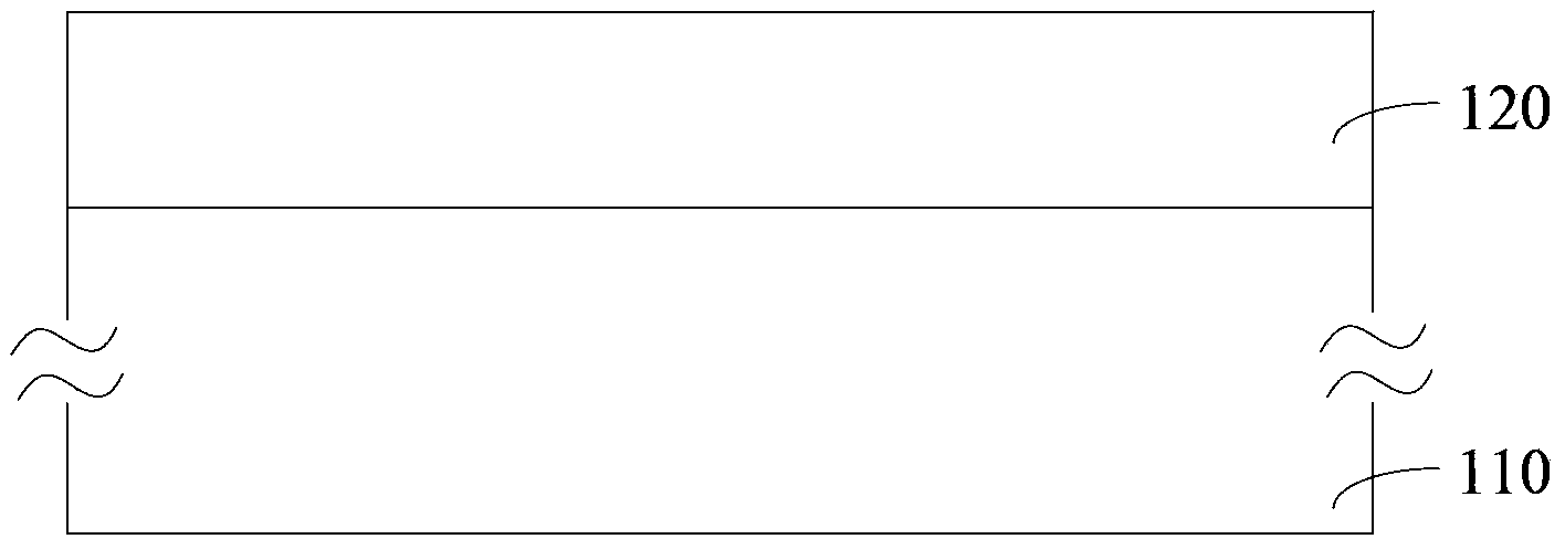
[0020] See Figure 2A , grow a thicker N-type buffer epitaxial layer 120 on the N+ substrate 110 .

[0021] S12, forming a P-type doped region in the buffer epitaxial layer by photolithography and ion implantation.

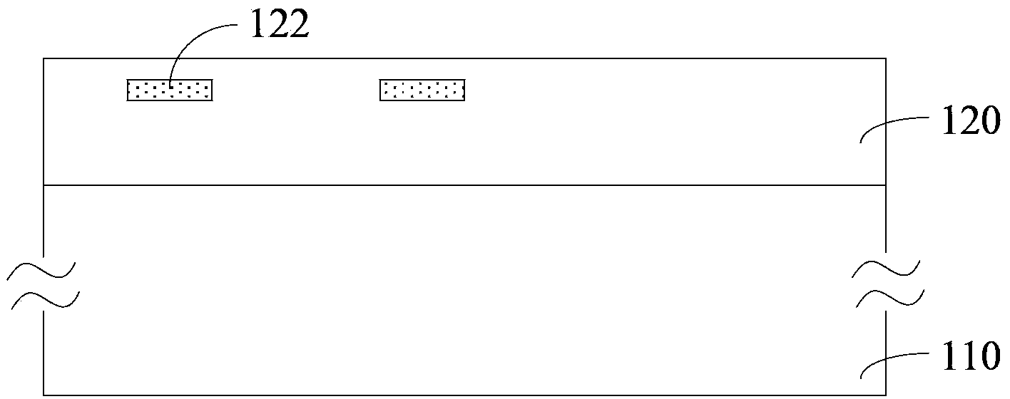
[0022] See Figure 2B , form the doped region window by photolithography and form the P-type doped region 122 by ion implantation (the photoresist is in Figure 2B not shown). It can be understood that in an actual device, multiple doped regions 12...


PUM


Abstract

The invention discloses a semiconductor device with a multi-layer epitaxial super junction framework. The semiconductor device comprises a first doping type substrate and a first doping type multi-layer epitaxial layer on the substrate, wherein a second doping type columnar structure is longitudinally formed in the multi-layer epitaxial layer; the multi-layer epitaxial layer comprises a buffering epitaxial layer and a plurality of normal epitaxial layers; and the thicknesses of the buffering epitaxial layer and the normal epitaxial layers are gradually decreasing from the buffering epitaxial layer up. The invention further discloses a manufacturing method of the semiconductor device with the multi-layer epitaxial super junction framework. According to the semiconductor device and the manufacturing method, the number of the epitaxial layers is reduced effectively; the production cycle and the cost are reduced; and stored charge of a body diode during working of the device is reduced and the reverse recovery time is shortened by controlling impurity distribution and corresponding junction depth.

Description

technical field [0001] The present invention relates to a method for manufacturing a semiconductor device, in particular to a semiconductor device with a multilayer epitaxial super junction structure, and also to a method for manufacturing a semiconductor device with a multilayer epitaxial super junction structure. Background technique [0002] The current super junction (Super Junction) architecture mainly includes two categories, one is to perform photolithography and implant P-type impurities after epitaxy, and repeat the process many times to obtain NP-staggered super junction columns; Thick N-type epitaxial layer, and then etch in the epitaxial layer to obtain deep trenches, and then form P-type silicon in the trenches, so as to obtain a similar super junction structure. [0003] For the former super junction structure, there is a body diode inside it, and the reverse recovery characteristic of the device is poor due to the high reverse recovery charge Qrr stored therei...

Claims


Application Information

Patent Timeline
IPC IPC(8): H01L21/265H01L29/06
CPCH01L21/266H01L29/0634
Inventor 俞义长孙晓儒殷允超周宏伟
Owner WUXI CHINA RESOURCES MICROELECTRONICS
Why Eureka
Try Eureka