Thyristor with buffer layer structure

A buffer layer, thyristor technology, applied in the direction of thyristor, electrical components, circuits, etc., can solve the problem of increased power loss of devices, and achieve the effect of reducing on-state voltage drop, improving on-state capability, and optimizing internal structure

Inactive Publication Date: 2013-10-30
HUBEI TECH SEMICON
View PDF4 Cites 0 Cited by
  • Summary
  • Abstract
  • Description
  • Claims
  • Application Information

AI Technical Summary

Problems solved by technology

If the minority carrier lifetime is reduced by technological means, although the switching speed can be increased, the power loss of the device will also be significantly increased.

Method used


Image

  • Thyristor with buffer layer structure
  • Thyristor with buffer layer structure
  • Thyristor with buffer layer structure

Examples


Embodiment Construction

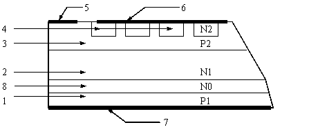
[0014] like figure 2 shown. The buffer layer structure thyristor of the present invention includes a tube shell and a PNPN four-layer three-terminal structure semiconductor chip packaged in the tube shell, and the four layers are P1 anode area 1, N1 long base area 2, cathode end P2 area 3 and N2 cathode area 4. The three terminals are anode A, cathode K and gate G. The junction depth of P1 anode region 1 is 15-50 μm; the junction depth of P2 region 3 at the cathode end is 45-130 μm; the thickness of N1 long base region 2 is 100-500 μm; the thickness of buffer layer N0 region 8 is 10-60 μm. The impurity concentration of the N0 region 8 of the buffer layer is higher than that of the N1 long base region 2 but lower than that of the P1 anode region 1 . The N0 region 8 of the buffer layer is formed by impurity diffusion, and may also be formed by epitaxy.

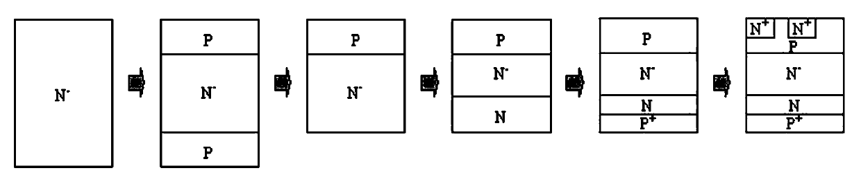
[0015] The silicon chip manufacturing process flow chart of thyristor with buffer layer structure is as follows image 3 ...


PUM


Abstract

The invention relates to a thyristor with a buffer layer structure, and belongs to the technical field of power semiconductor devices. The thyristor mainly solves the problem that when an existing thyristor is applied to a high frequency high-power current transforming power source and an impulse-power power source, the existing thyristor is large in pressure drop, low in communciating speed and the like. The thyristor is mainly characterized by comprising a thyristor shell and a semiconductor chip which is of a PNPN four-layer three-end structure and packaged in the thyristor shell. A buffer layer N0 zone is additionally arranged between a P1 zone and an N1 zone of the semiconductor chip, the surface concentration of the N1 zone is 10-200 times higher than that of the N0 zone, and the surface concentration of the N1 zone is 50-500 times lower than that of the P1 zone. The thyristor has the advantages that when the thyristor is applied to the high frequency high-power current transforming power source and the impulse-power power source, the on-state voltage drop can be obviously reduced, therefore, the on-state capacity and the operational reliability can be improved, meanwhile, the internal structure can be optimized, the large-charging storage electric charge is reduced, and the recovery softness is improved. The thyristor is mainly applied to high-power impulse power source devices.

Description

technical field [0001] The invention belongs to the technical field of power semiconductor devices. It specifically relates to a semiconductor switching device, which is mainly used in high-power variable current power supplies, especially high-power pulse power supplies. Background technique [0002] A thyristor is a semiconductor device with a PNPN four-layer three-terminal structure. The usual manufacturing method is to simultaneously perform P-type doping on both ends of the N-type silicon wafer, and first form a symmetrical PNP structure. Then perform N-type selective diffusion doping in the P region of the cathode end, and finally form a PNPN structure, such as figure 1 . The doping junction depth and impurity concentration distribution of the P1 anode region and the P2 cathode end region are the same, and the N1 long base region layer is thicker. N2 is the cathode area. [0003] In some electrical systems that require fast turn-on and fast turn-off, the thyristor...

Claims


Application Information

Patent Timeline
Patent Type & Authority Applications(China)
IPC IPC(8): H01L29/74H01L29/08
Inventor 张桥颜家圣刘小俐杨宁
Owner HUBEI TECH SEMICON
Why Eureka
Try Eureka